
| CAD Model: | View CAD Model |
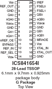
| Pkg. Type: | TSSOP |
| Pkg. Code: | DQG28 |
| Lead Count (#): | 28 |
| Pkg. Dimensions (mm): | 9.7 x 6.1 x 1.0 |
| Pitch (mm): | 0.65 |
| Moisture Sensitivity Level (MSL) | 3 |
| Pb (Lead) Free | Yes |
| ECCN (US) | EAR99 |
| HTS (US) | 8542.39.0090 |
| Lead Count (#) | 28 |
| Carrier Type | Reel |
| Moisture Sensitivity Level (MSL) | 3 |
| Qty. per Reel (#) | 1000 |
| Qty. per Carrier (#) | 0 |
| Pb (Lead) Free | Yes |
| Pb Free Category | e3 Sn |
| Temp. Range (°C) | -40 to 85°C |
| Advanced Features | Reference Output |
| App Jitter Compliance | PCIe |
| C-C Jitter Max P-P (ps) | 35 |
| Core Voltage (V) | 3.3 |
| Feedback Input | No |
| Input Freq (MHz) | 25 - 25 |
| Input Type | Crystal, LVCMOS |
| Inputs (#) | 2 |
| Length (mm) | 9.7 |
| MOQ | 1000 |
| Output Banks (#) | 3 |
| Output Freq Range (MHz) | 100 - 100, 125 - 125 |
| Output Skew (ps) | 100 |
| Output Type | HCSL, LVCMOS |
| Output Voltage (V) | 3.3 |
| Outputs (#) | 5 |
| Package Area (mm²) | 47 |
| Phase Jitter Typ RMS (ps) | 0.44 |
| Pitch (mm) | 0.65 |
| Pkg. Dimensions (mm) | 9.7 x 6.1 x 1.0 |
| Pkg. Type | TSSOP |
| Product Category | FemtoClock, Low Jitter Clocks (<700 fs RMS) |
| Prog. Clock | No |
| Reel Size (in) | 13 |
| Reference Output | Yes |
| Requires Terms and Conditions | Does not require acceptance of Terms and Conditions |
| Spread Spectrum | No |
| Tape & Reel | Yes |
| Thickness (mm) | 1 |
| Width (mm) | 6.1 |
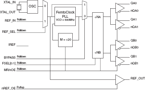
The 841654I is an optimized PCIe and sRIO clock generator. The device uses a 25MHz parallel crystal to generate 100MHz and 125MHz clock signals, replacing solutions requiring multiple oscillator and fanout buffer solutions. The device has excellent phase jitter (< 1ps rms) suitable to clock components requiring precise and low-jitter PCIe or sRIO or both clock signals. Designed for telecom, networking and industrial applications, the 841654I can also drive the high-speed sRIO and PCIe SerDes clock inputs of communication processors, DSPs, switches and bridges.