
Features
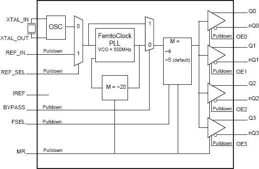
- Four 0.7V differential HCSL outputs: configurable for PCIe (100MHz) and sRIO (125MHz) clock signals
- Selectable crystal oscillator interface, 25MHz, 18pF parallel resonant crystal or LVCMOS/LVTTL single-ended reference clock input
- Supports the following output frequencies: 100MHz or 125MHz
- VCO: 500MHz
- PLL bypass and output enable
- RMS phase jitter @ 125MHz, using a 25MHz crystal (1.875MHz - 20MHz): 0.5ps (typical)
- PCI Express® (2.5 Gb/S), Gen 2 (5 Gb/s) and Gen 3 (8 Gb/s) jitter compliant
- Full 3.3V operating supply
- -40°C to 85°C ambient operating temperature
- Available in lead-free (RoHS 6) package

Description
The 841604I-01 is an optimized PCIe and sRIO clock generator. The device uses a 25MHz parallel crystal to generate 100MHz and 125MHz clock signals, replacing solutions requiring multiple oscillator and fanout buffer solutions. The device has excellent phase jitter (< 1ps rms) suitable to clock components requiring precise and low-jitter PCIe or sRIO or both clock signals. Designed for telecom, networking and industrial applications, the 841604I-01 can also drive the high-speed sRIO and PCIe SerDes clock inputs of communication processors, DSPs, switches and bridges.