
Features
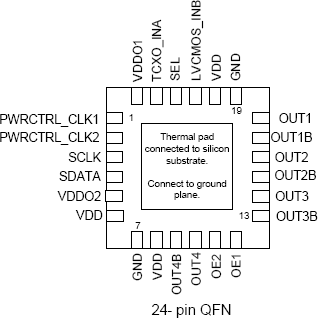
- Packaged in 24-pin QFN
- TCXO sine wave input
- +2.5 V operating voltage
- Four buffered LVDS outputs
- Two programmable outputs for power control up to 3.0 V LVCMOS levels based on VDDO1/VDDO2
- Individual output enables controlled via I2C or OEx
- Pb-free, RoHS compliant package
- Industrial temperature range (-40°C to +85°C)
Description
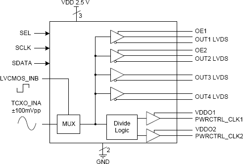
The IDT6T39007A is a low-power, four output clock distribution circuit. The device takes a TCXO or 1.8 V to 2.5 V LVCMOS input and generates four high-quality LVDS outputs, and two programmable divided outputs. It includes a redundant input with automatic glitch-free switching when the primary reference is removed. The primary input may be selected by the user by pulling the SEL pin low or high. If the primary input is removed and brought back, it will not be re-selected until 1024 cycles have passed. The IDT6T39007A specifically addresses the needs of handheld applications in both performance and package size. The device is packaged in a small 4mm x 4mm 24-pin QFN, allowing optimal use for limited board space.