
Overview
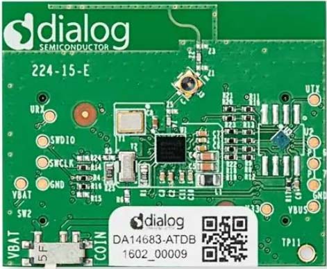
The DA14683 Development Kit Pro is ideal for software developers who want total control over their software development and want to keep an eye on the power consumption of their application. The kit contains a motherboard and an extra DA14683 Bluetooth® Low Energy WL-CSP5 daughterboard (DA14683-00U2DB-P), and gives you access to all of the package’s general-purpose input-outputs (GPIOs). With the RF connector on the daughterboard, you can perform the RF measurements. The kit's on-board Segger chip gives you complete debugging capability. In addition, the dedicated on-board circuitry allows you, in combination with our complete software environment SmartSnippets™ Studio, to profile and fine-tune the power consumption of your application to get the most out of the DA14683's advantages.
Features
- Highly integrated DA1468x SoC supported
- DA1468x System-on-Chip (SoCs) can be accessed over UART and/or JTAG with no additional external hardware
- Access to all GPIOs provided from the chip reset push button
- General-purpose LED and push button
- White LED connected to dedicated PWM pin (LED1 pin)
- Current monitoring circuit associated with appropriate software on PC
- Powered from either USB2(DBG) connector or Li-Po battery
- JTAG and UART interface over USB2 (DBG) connector for development purposes
- Option for Coin-Cell battery on the daughterboard (non-rechargeable, no current monitored)
- Dedicated USB (USB1-CHG) connector for charging a Li-Po battery
- DA1468x different package easily replaceable by replacing the daughterboard
- QSPI flash on daughterboard
- 2.4GHz printed inverted-F antenna on the daughterboard
- RF mechanical switch for conducted RF measurements on the daughterboard
- Breakout headers with clearly marked signals
- 16MHz system and 32.768KHz low-power crystals on the daughterboard
- Fixed 3.0V/1.8V and a variable (1.9V to 4.3V) low-dropout regulator (LDO) power options

Sample & Buy
DA14683-00U2DB-P
Active| MOQ: | 1 |
| SPQ: | 1 |
| Pb (Lead) Free: | Yes |
| Carrier Type: | Box |
| Assembly Location: | GERMANY |
Resources
Support
Support Communities
- Customize ATT_MTU on DA14683
Hello, We are evaluating DA14683 on the data throughput by the DA14683-00U2DB-P Development Kit. We want to increase the default ATT_MTU from 23 to 283. We modify the ble_peripheral demo project and customize the BLE initialization as: ble_peripheral_start(); ble_register_app(); ble_gap_mtu ...
Sep 18, 2021

Support Communities

