
Features
- Additive PCIe Gen 5 CC jitter < 60fs RMS (Fanout mode)
- PCIe Gen 5 CC jitter < 150fs RMS (High-BW Zero-Delay Buffer (ZDB) mode)
- 8 Low Power HCSL (LP-HCSL) outputs eliminate 4 resistors per output pair
- Direct connection to 85Ω transmission lines
- Dedicated OE# pin for each output
- Spread spectrum tolerant
- Pin or SMBus configuration
- 3 selectable SMBus addresses
- SMBus interface not required for device operation
- Easy AC coupling to other logic families, see application note AN-891.
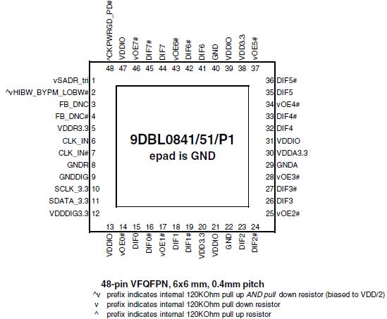
- Space-saving 48-pin 6mm × 6mm VFQFPN
Description
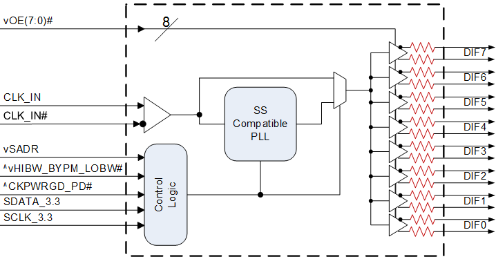
The 9DBL0851 8-output 3.3V PCIe zero-delay/fanout buffer supports PCIe Gen 1 through Gen 5 and both Common and Independent Reference Clock architectures.
For information regarding evaluation boards and material, please contact your local sales representative.
Parameters
| Attributes | Value |
|---|---|
| Diff. Outputs | 8 |
| Diff. Output Signaling | LP-HCSL |
| Output Freq Range (MHz) | 1 - 200 |
| Diff. Inputs | 1 |
| Diff. Input Signaling | HCSL |
| Accepts Spread Spec Input | Yes |
| Power Consumption Typ (mW) | 211 |
| Supply Voltage (V) | 3.3 - 3.3 |
| Output Type | LP-HCSL |
| Diff. Termination Resistors | 0 |
| Package Area (mm²) | 36 |
| Battery Backup | No |
| Battery Seal | No |
| CPU Supervisory Function POR | No |
| Crystal Frequency Trimming | No |
| Frequency Out Pin | No |
| Inputs (#) | 1 |
| Input Freq (MHz) | 1 - 200 |
| Additive Phase Jitter Typ RMS (fs) | 300 |
| Function | Zero Delay Buffer |
| Input Type | HCSL |
| Output Banks (#) | 1 |
| Core Voltage (V) | 3.3 |
| Output Voltage (V) | 0.8 |
| Product Category | PCI Express Clocks |
Package Options
| Pkg. Type | Pkg. Dimensions (mm) | Lead Count (#) | Pitch (mm) |
|---|---|---|---|
| VFQFPN | 6.0 x 6.0 x 0.9 | 48 | 0.4 |
Complete Your Design
Explore complementary products to elevate your design
| Part Number | Status | Samples | Longevity | Stock | Package | Budgetary Price (USD) | Lead Count (#) | Carrier Type | Moisture Sensitivity Level (MSL) | Qty. per Reel (#) | Qty. per Carrier (#) | Pb (Lead) Free | Pb Free Category | Temp. Range (°C) | Country of Assembly | Country of Wafer Fabrication |
|---|---|---|---|---|---|---|---|---|---|---|---|---|---|---|---|---|
| 9DBL0851CKILF | Active | Available | 2040 Apr | Out of Stock | VFQFPN | 1ku | $1.62 | 48# | Tray | 3 | 0 | 490# | Yes | e3 Sn | -40 to 85°C | CHINA | TAIWAN |
| 9DBL0851CKILFT | Active | N/A | 2040 Apr | Out of Stock | VFQFPN | 1ku | $1.62 | 48# | Reel | 3 | 2500# | 0 | Yes | e3 Sn | -40 to 85°C | CHINA | TAIWAN |
| 9DBL0851BKILF | Obsolete | N/A | Out of Stock | VFQFPN | 48# | Tray | 3 | 0 | 490# | Yes | e3 Sn | -40 to 85°C | ||||
| 9DBL0851BKILFT | Obsolete | N/A | Out of Stock | VFQFPN | 48# | Reel | 3 | 2500# | 0 | Yes | e3 Sn | -40 to 85°C |
Complete Your Design
Explore complementary products to elevate your design
Filters
Applied Filters
- DatasheetPDF 570 KB R31DS0116EU0105 Rev.1.05 Nov 05, 2025
- Application NotePDF 431 KB 7WDXRDKU4E7E-5-59216 Dec 06, 2023
- Product AdvisoryPDF 171 KB Dec 20, 2022
- Product Change NoticePDF 734 KB Nov 16, 2022
- Product Change NoticePDF 728 KB May 13, 2022
- Application NotePDF 235 KB 7WDXRDKU4E7E-5-58851 Apr 08, 2015
- Application NotePDF 1.9 MB 7WDXRDKU4E7E-5-57315 May 13, 2014
- Application NotePDF 495 KB 7WDXRDKU4E7E-5-57312 May 12, 2014
- Application NotePDF 442 KB 7WDXRDKU4E7E-5-57298 May 08, 2014
- Application NotePDF 120 KB 7WDXRDKU4E7E-5-57289 May 06, 2014
- DatasheetPDF 570 KB R31DS0116EU0105 Rev.1.05 Nov 05, 2025
Recommended Documents (2)
- DatasheetPDF 570 KB R31DS0116EU0105 Rev.1.05 Nov 05, 2025
Datasheets (2)
Manuals & Guides (1)
- Application NotePDF 431 KB 7WDXRDKU4E7E-5-59216 Dec 06, 2023
- Application NotePDF 1.99 MB 7WDXRDKU4E7E-5-57242 Mar 01, 2022
- Application NotePDF 235 KB 7WDXRDKU4E7E-5-58851 Apr 08, 2015View More (13)
Application Notes & White Papers (13)
- Product AdvisoryPDF 171 KB Dec 20, 2022
- Product Change NoticePDF 734 KB Nov 16, 2022
- Product Change NoticePDF 728 KB May 13, 2022
- Product Change NoticePDF 983 KB Jun 25, 2019View More (6)
Product Notices (PCN, EOL, etc) (6)
No Results Found.
Make sure all keywords are spelled correctly.
Try fewer, different, or more general terms to vary your search.
If you have filters applied, consider deselecting some to broaden your results.
- Search our extensive knowledgebase, designed to help customers with their FAQs.
- Get help from our expert Renesas technical staff and community on our support forums.
No Results Found.
Make sure all keywords are spelled correctly.
Try fewer, different, or more general terms to vary your search.
If you have filters applied, consider deselecting some to broaden your results.
- Search our extensive knowledgebase, designed to help customers with their FAQs.
- Get help from our expert Renesas technical staff and community on our support forums.
Schematics & Design Files (1)
No Results Found.
Make sure all keywords are spelled correctly.
Try fewer, different, or more general terms to vary your search.
If you have filters applied, consider deselecting some to broaden your results.
- Search our extensive knowledgebase, designed to help customers with their FAQs.
- Get help from our expert Renesas technical staff and community on our support forums.
No Results Found.
Make sure all keywords are spelled correctly.
Try fewer, different, or more general terms to vary your search.
If you have filters applied, consider deselecting some to broaden your results.
- Search our extensive knowledgebase, designed to help customers with their FAQs.
- Get help from our expert Renesas technical staff and community on our support forums.
No Results Found.
Make sure all keywords are spelled correctly.
Try fewer, different, or more general terms to vary your search.
If you have filters applied, consider deselecting some to broaden your results.
- Search our extensive knowledgebase, designed to help customers with their FAQs.
- Get help from our expert Renesas technical staff and community on our support forums.
Marketing Collateral (1)
No Results Found.
Make sure all keywords are spelled correctly.
Try fewer, different, or more general terms to vary your search.
If you have filters applied, consider deselecting some to broaden your results.
- Search our extensive knowledgebase, designed to help customers with their FAQs.
- Get help from our expert Renesas technical staff and community on our support forums.
No Results Found.
Make sure all keywords are spelled correctly.
Try fewer, different, or more general terms to vary your search.
If you have filters applied, consider deselecting some to broaden your results.
- Search our extensive knowledgebase, designed to help customers with their FAQs.
- Get help from our expert Renesas technical staff and community on our support forums.
No Results Found.
Make sure all keywords are spelled correctly.
Try fewer, different, or more general terms to vary your search.
If you have filters applied, consider deselecting some to broaden your results.
- Search our extensive knowledgebase, designed to help customers with their FAQs.
- Get help from our expert Renesas technical staff and community on our support forums.
Filters
Applied Filters
Software & Tools
Filter by Type
Filter by Provider
Sample Code
Filter by Application
Filter by Function
Filter by Compiler
Filter by IDE
Simulation Models
Partner Solutions
No Results Found.
Make sure all keywords are spelled correctly.
Try fewer, different, or more general terms to vary your search.
If you have filters applied, consider deselecting some to broaden your results.
- Search our extensive knowledgebase, designed to help customers with their FAQs.
- Get help from our expert Renesas technical staff and community on our support forums.
Software & Tools (1)
No Results Found.
Make sure all keywords are spelled correctly.
Try fewer, different, or more general terms to vary your search.
If you have filters applied, consider deselecting some to broaden your results.
- Search our extensive knowledgebase, designed to help customers with their FAQs.
- Get help from our expert Renesas technical staff and community on our support forums.
Simulation Models (1)
No Results Found.
Make sure all keywords are spelled correctly.
Try fewer, different, or more general terms to vary your search.
If you have filters applied, consider deselecting some to broaden your results.
- Search our extensive knowledgebase, designed to help customers with their FAQs.
- Get help from our expert Renesas technical staff and community on our support forums.
A detailed overview of IDT's full-featured PCI Express (PCIe) clock and timing solutions. The presentation addresses PCIe Gen 1, Gen 2, Gen 3, and Gen 4 architectures and how IDT's industry-leading solutions provide all the functions, features, and performance required by the application.
Presented by Ron Wade, System Architect at IDT. For more information visit the PCIe clocks page.
This is the first video in our PCIe series. In this video, we define PCIe architectures, focusing on common and separate clock architectures. Watch the rest of the video series below where Ron will cover the impact of different timing architectures.
In this episode, Ron Wade from IDT (acquired by Renesas) explains PCIe common clocking and its impact on timing solutions. Learn about using a single clock source, fan-out buffers, and the considerations for spread spectrum and non-spread spectrum clocking in PCIe systems.
In this video, we explore PCIe with separate reference clocks and the effects of clock selection. Learn how separate reference clocks work and their impact on system performance and stability.
This video provides a high-level overview of Separate Reference Clock with Independent Spread (SRIS) architectures for PCI Express systems, additional performance requirements that this clocking architecture imposes on the reference clocks, and some system implications encountered trying to implement the architecture.
An overview of IDT's full-featured PCI Express (PCIe) clock zero-delay buffers and fanout buffers addressing PCIe Gen 1, Gen 2, Gen 3, and Gen 4.
Presented by Ron Wade, System Architect at IDT.
An overview of PCI Express applications and how IDT's industry-leading portfolio of PCIe clock products addresses the requirements. The video briefly discusses PCIe riser cards, embedded SOC, and PCIe storage (NVME) examples.
Presented by Ron Wade, System Architect at IDT.
A brief overview of how data rates have changed from PCI Express (PCIe) Generation 1, Gen 2, Gen 3, Gen 4 and Gen 5.
Presented by Ron Wade, system architect at IDT.
A brief overview of how clock and timing specifications have changed from PCI Express (PCIe) Generation 1, Gen 2, Gen 3, Gen 4 and Gen 5.
Presented by Ron Wade, system architect at IDT (acquired by Renesas).
A brief overview of the PCI Express common clock (CC) jitter model, and the transfer functions as they relate to the timing PLLs. This model applies to PCI Express (PCIe) Gen 2, Gen 3, Gen 4 and Gen 5. The equations would be slightly different for other PCIe architectures, such as SRIS, SRnS, or data clocked.
Presented by Ron Wade, system architect at IDT (acquired by Renesas). For more information about Renesas's PCIe timing solutions, visit the PCI Express (PCIe) Clocks page.

Support Communities


