

| CAD Model: | View CAD Model |
| Pkg. Type: | FCCSP |
| Pkg. Code: | BV0264AA |
| Lead Count (#): | 264 |
| Pkg. Dimensions (mm): | 8.7 x 14.4 x 0.9 |
| Pitch (mm): | 0.6 |
| Moisture Sensitivity Level (MSL) | 3 |
| Pb (Lead) Free | Yes |
| ECCN (US) | |
| HTS (US) |
| Pkg. Type | FCCSP |
| Lead Count (#) | 264 |
| Carrier Type | Tray |
| Moisture Sensitivity Level (MSL) | 3 |
| Qty. per Reel (#) | 0 |
| Qty. per Carrier (#) | 170 |
| Pb (Lead) Free | Yes |
| Pb Free Category | e8 SnAgCu |
| Temp. Range (°C) | 0 to 70°C |
| Application System | Server |
| Function | DDR5 Gen 5.0 Server RCD |
| Input Voltage Range (V) | 1.06 - 1.16 |
| Length (mm) | 8.7 |
| MOQ | 340 |
| Pitch (mm) | 0.6 |
| Pkg. Dimensions (mm) | 8.7 x 14.4 x 0.9 |
| Product Type | Registering Clock Driver |
| Tape & Reel | No |
| Thickness (mm) | 0.9 |
| Width (mm) | 14.4 |
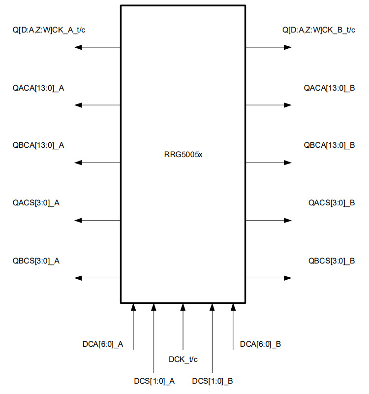
The RRG5005x-B08 is a registering clock driver (RCD) used on DDR5 RDIMMs. Its primary function is to buffer the Command/Address (CA) bus, chip selects, and clock between the host controller and the DRAMs. The RRG5005x-B08 contains two separate channels, which have some common logic such as clocking, but otherwise operate independently of each other. Each channel has a 7-bit double data rate CA bus input, a single parity input, two chip select inputs, and produces two copies of 14-bit single data rate CA bus outputs, and two copies of the chip select outputs. The RCD has a common clock input and PLL, but produces four separate clock pairs to the DRAM channels.