Processor Core
All Synergy™ microcontrollers (MCUs) use 32-bit Arm® Cortex®-M CPU processor cores designed specifically for energy-efficient and cost-sensitive embedded applications.
The rich instruction architectures of these cores are upward compatible, driving scalability and a high degree of code re-use. Compact Thumb instructions, sophisticated power management with multiple sleep modes, fast interrupt handling, and deep visibility inside the CPU core for debugging, create a reliable foundation for IoT and embedded products.
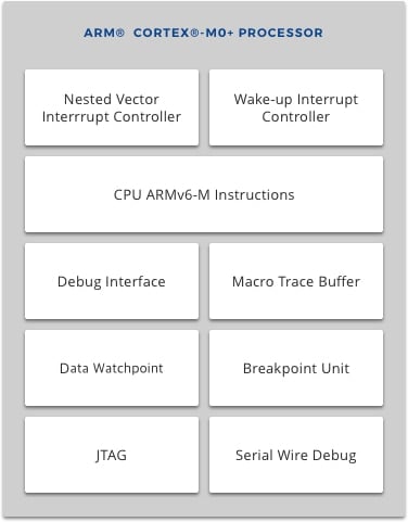
Arm Cortex-M0+
The ultra-low power Arm Cortex-M0+ core is the most energy-efficient Arm processor available.
Combining several low power modes and flexible power control over system components, the 32-bit Arm Cortex-M0+ is ideal for applications requiring long battery life. Fast code execution permits longer sleep time, while optimized code fetching reduces flash and ROM power consumption. The processor enables full system-level debug, while an integrated interrupt controller provides deterministic interrupt handling, enabling a fast response to real-time events. The processor is upward compatible with other Cortex-M processors, providing enhanced scalability and code re-usability.
Debug
The processor leverages the proven CoreSight™ architecture to provide full system-level debug access.
The system includes a Debug Access Port (DAP) with a 12.5MHz serial wire debug interface and a built-in Micro Trace Buffer (MTB) with 1KB of SRAM for capturing program flow trace data. Debug registers provide system reset and halt control.
NVIC
The processor features a versatile, built-in Nested Vectored Interrupt Controller (NVIC) that supports up to 32 external interrupts and includes dedicated Non-Maskable Interrupt (NMI).
External interrupts support up to four priority levels and can be triggered by pulse or level events. NVIC also supports relocating the vector table for additional flexibility.
Arm Cortex-M0+ is available on low power Synergy S124 and S128 MCUs.
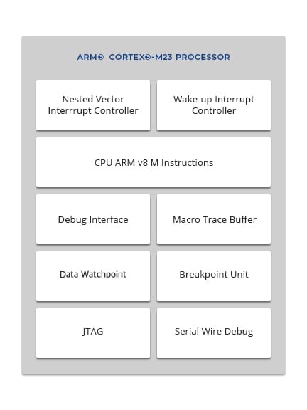
Arm Cortex-M23
The Arm Cortex-M23 core is the energy-efficient Arm processor optimized for ultra-low power. The Cortex-M23 processor is very compact and supports the Armv8-M baseline instruction, which has high code density with 32-bit performance. The processor provides hardware division instruction for faster integer operation and Armv8 Protected Memory System Architecture (PMSA).
The processor is upward compatible with other Cortex-M processors, providing enhanced scalability and code re-usability.
Debug
The processor leverages the proven CoreSight architecture to provide full system-level debug access.
The system includes a debug access port (DAP) with a 12.5MHz serial wire debug interface and a built-in Micro Trace Buffer (MTB) with 1KB of SRAM for capturing program flow trace data. Debug registers provide system reset and halt control.
NVIC
The processor features a versatile, built-in Nested Vectored Interrupt Controller (NVIC) that supports up to 32 external interrupts and includes dedicated Non-Maskable Interrupt (NMI).
Arm Cortex-M23 is available on the low power Synergy S1JA MCUs.
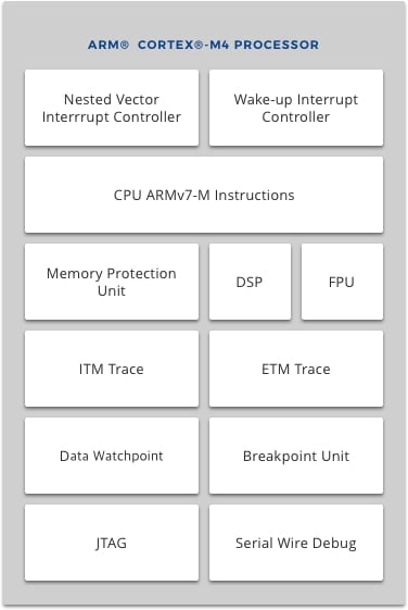
Arm Cortex-M4
The Arm Cortex-M4 core offers a combination of control and signal processing capabilities while delivering low dynamic current consumption.
The processor features Thumb instruction support and bit-banding capability for faster data manipulation. An integrated Floating Point Unit (FPU) accelerates single-precision operations, providing faster processing and reduced CPU load. Integrated sleep and output retention modes offer significant power savings, with additional flexibility to power down unused peripherals.
Debug
The processor leverages the proven CoreSight architecture, providing access to all system memory and registers, internal core registers, and memory-mapped devices.
There are two Debug Access Ports (DAP) with both JTAG and serial wire access, along with multiple CoreSight components for advanced trace capabilities. It also features flash patch and breakpoint capabilities for advanced debugging.
NVIC and ARM MPU
The processor features a Nested Vectored Interrupt Controller (NVIC) and a Memory Protection Unit (MPU).
The configurable NVIC handles up to 240 interrupts and optimizes for low-latency exception and interrupt handling. It can also be used to wake the processor from sleep modes.
The MPU enforces access and privilege rules, offering eight protection regions with various priority levels. The MPU generates a fault if memory is accessed without the appropriate permissions.
Trace
The processor features several components to provide advanced tracing capabilities.
The Data Watchpoint and Trace (DWT) unit configures watchpoints and triggers, while the Embedded Trace Macrocell (ETM) reconstructs program flow and stores trace data into the Embedded Trace Buffer (ETB). The Instrumentation Trace Macrocell (ITM) supports printf-style debugging for operating system and application events and generates diagnostic system information.
Arm Cortex-M4 is available on the following Synergy MCUs.
S3 Series (High Efficiency): S3A1, S3A3, S3A7, S3A6
S5 Series (High Integration): S5D3, S5D5, S5D9
S7 Series (High Performance): S7G2
Memory
Synergy MCUs offer advanced memory features for greater design and development flexibility, and provide enhanced protection against unauthorized or unintentional access.
The Memory Protection Unit (MPU) safeguards designated regions of memory from unauthorized read or write attempts. The Memory Mirror Function (MMF) provides the flexibility to virtually re-map the address of sections of code flash to facilitate robust firmware updates. A memory bus allows the MCU to access external memory and devices.
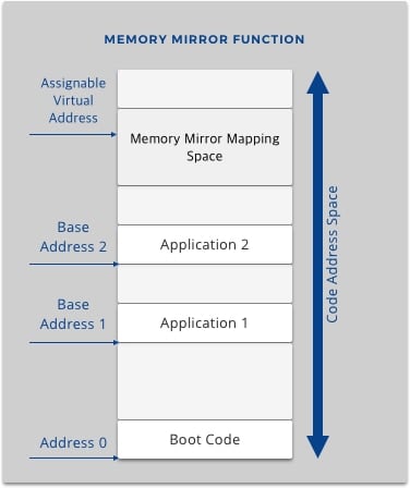
Memory Mirror Function (MMF)
Enables a convenient means to virtually re-map boot code or application code to a different physical address in code flash memory space.
The dedicated 8MB space for the memory mirror function is used to safely re-map boot code after a firmware update, or to virtually map multiple applications to a common virtual address. Application code is developed based on the virtual address and does not require awareness of the actual physical address in code flash.
MMF is available on the following Synergy MCUs.
S1 Series (Low Power): S1JA
S3 Series (High Efficiency): S3A1, S3A3, S3A7
S5 Series (High Integration): S5D3, S5D5, S5D9
S7 Series (High Performance): S7G2
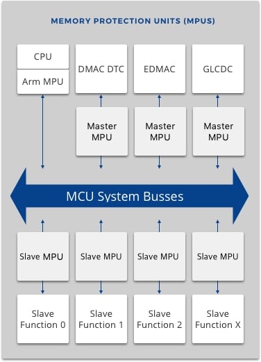
Memory Protection Units (MPUs)
Safeguard against unauthorized access to memory by preventing unwanted dynamic access by other bus masters. These MPUs are in addition to the Arm MPU that is included within the Arm Cortex-M CPU core.
Three types of MPUs are included: Bus Master MPU, Bus Slave MPU and Security MPU. The Bus Master MPU protects against reads and writes from unauthorized bus masters for up to 32 regions of memory, while the Bus Slave MPU protects access to bus slave functions such as flash, SRAM or peripherals. The Security MPU provides additional protection against access to designated memory, data or peripherals by untrusted code.
MPUs are available on the following Synergy MCUs.
S1 Series (Low Power): S128, S1JA
S3 Series (High Efficiency): S3A1, S3A3, S3A6, S3A7
S5 Series (High Integration): S5D3, S5D5, S5D9
S7 Series (High Performance): S7G2
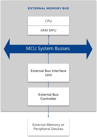
External Memory Bus
Allows the CPU and DMA to access external physical devices, such as external memory or peripherals.
External address space is divided into multiple chip select areas, with each area offering independent configuration for 8- or 16-bit bus width and endian mode. The external bus speed can operate at speeds up to 120MHz, depending on the MCU series and operating conditions.
External Memory Bus is available on the following Synergy MCUs.
S3 Series (High Efficiency): S3A1, S3A3, S3A7
S5 Series (High Integration): S5D3, S5D5, S5D9
S7 Series (High Performance): S7G2
Analog
Synergy MCUs provide a range of analog signal processing and generation capabilities, including A/D conversion, D/A conversion and analog signal comparison.
The Event Link Controller (ELC), PWM, external triggers, or software can trigger signal processing actions. Built-in diagnostics ensure reliable performance and synchronization features offer protection against noise interference between modules. Synergy MCUs also include integrated amplifiers that provide the ability to drive external loads.
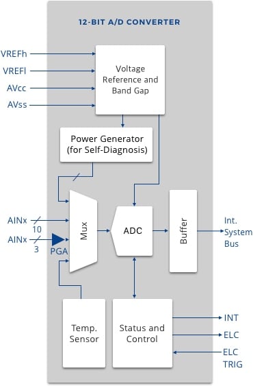
12-Bit A/D Converter (ADC12)
Converts analog voltages from up to 25 external inputs, an internal temperature sensor, and an internal reference voltage, all at a rate of 0.4µsec per channel.
The ADC12 supports the following operating modes:
- Single Scan – conversion is performed once on selected sources
- Continuous Scan – conversion is performed repeatedly on selected sources
- Group Scan – allows grouping of sources for independent start triggers
The ADC12 can be triggered from multiple internal and external sources, such as external trigger pins, ELC, PWM, or software. Built-in ADC diagnostics verify the module’s functionality at the beginning of each scan, ensuring accurate conversion values.
ADC12 is available on the following Synergy MCUs.
S5 Series (High Integration): S5D3, S5D5, S5D9
S7 Series (High Performance): S7G2
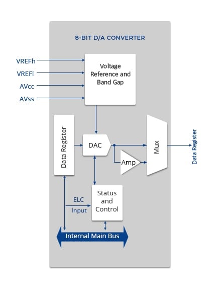
8-Bit D/A Converter (DAC8)
Converts digital values to analog voltages for a variety of application uses.
The DAC8 contains an integrated output amplifier for driving external loads, and can be synchronized to avoid interference with the A/D Converter (ADC). It uses both internal and external reference voltages to ensure accurate conversions. Conversions can be triggered from other system events using the ELC.
DAC8 is available on the following Synergy MCUs.
S1 Series (Low Power): S1JA
S3 Series (High Efficiency): S3A1
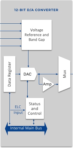
12-Bit D/A Converter (DAC12)
Converts digital values to analog voltages for a variety of application uses.
The DAC12 contains an integrated output amplifier for driving external loads and can be synchronized to avoid interference with the A/D Converter (ADC). It uses both internal and external reference voltages to ensure accurate conversions. Conversions can be triggered from other system events using the ELC.
DAC12 is available on the following Synergy MCUs.
S1 Series (Low Power): S124, S1JA
S3 Series (High Efficiency): S3A1, S3A3, S3A6, S3A7
S5 Series (High Integration): S5D3, S5D5, S5D9
S7 Series (High Performance): S7G2
14-Bit A/D Converter (ADC14)
Converts analog voltages from up to 28 external inputs, an internal temperature sensor and an internal reference voltage, all at a rate of 0.7µsec per channel.
- Single Scan – conversion is performed once on selected sources
- Continuous Scan – conversion is performed repeatedly on selected sources
- Group Scan – allows grouping of sources for independent start triggers
The ADC14 can be triggered from multiple internal and external sources, such as external trigger pins, ELC, PWM, or software. Built-in ADC diagnostics verify the module’s functionality at the beginning of each scan, ensuring accurate conversion values.
ADC14 is available on the following Synergy MCUs.
S1 Series (Low Power): S124, S128
S3 Series (High Efficiency): S3A1, S3A3, S3A6, S3A7
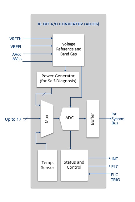
16-Bit A/D Converter (ADC16)
Converts analog voltages from up to 17 channels by single-ended input mode, up to 4 channels differential input mode, an internal temperature sensor, and an internal reference voltage, all at a rate of 0.82µsec per channel.
The ADC16 supports the following operating modes:
- Single Scan – conversion is performed once on selected sources
- Continuous Scan – conversion is performed repeatedly on selected sources
- Group Scan – allows grouping of sources for independent start triggers
The ADC16 can be triggered from multiple internal and external sources, such as external trigger pins, ELC, PWM, or software. Built-in ADC diagnostics verify the module’s functionality at the beginning of each scan, ensuring accurate conversion values.
ADC16 is available on the low power Synergy S1JA MCUs.
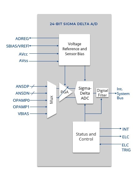
24-Bit Sigma-Delta A/D Converter (SDADC24)
The signal from an input multiplexer (single-ended input mode: up to 10 channels, differential input mode: up to 5 channels) is input to the 24-bit Sigma-Delta A/D converter via the programmable gain instrumentation amplifier (PGA). The A/D conversion result is filtered by the digital filter, and is then stored in an output register.
SDADC24 is available on the low power Synergy S1JA MCUs.
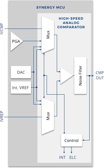
High-Speed Analog Comparator (ACMPHS)
Compares a test voltage with a reference voltage and provides a digital output based on the result of the conversion.
Both the test signal and the reference voltage signal can be supplied from internal sources, such as the DAC or internal reference voltage, as well as from external sources. This flexibility is beneficial in applications that require go/no-go comparisons to be performed between analog signals without requiring ADC conversion. An integrated noise filter provides protection from interference on the signal input lines.
ACMPHS is available on the following Synergy MCUs.
S1 Series (Low Power): S1JA
S3 Series (High Efficiency): S3A3, S3A7
S5 Series (High Integration): S5D3, S5D5, S5D9
S7 Series (High Performance): S7G2
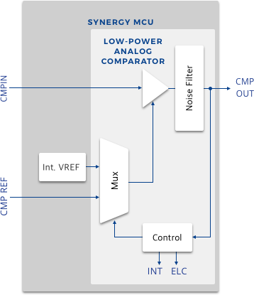
Low-Power Analog Comparator (ACMPLP)
Compares a test voltage with a reference voltage to provide a digital output based on the result of the conversion. The reference voltage can be supplied from internal sources, such as the DAC or internal reference voltage, as well as from external sources. This flexibility is beneficial in applications that require go/no-go comparisons to be performed between analog signals without requiring ADC conversion. An integrated noise filter provides protection from interference on the signal input lines.
ACMPLP is available on the following Synergy MCUs.
S1 Series (Low Power): S124, S128, S1JA
S3 Series (High Efficiency): S3A1, S3A3, S3A6, S3A7
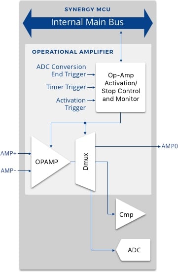
Operational Amplifier (OPAMP)
Conditions and amplifies analog input signals before sending to the High-Speed Analog Comparator (ACMPHS) or A/D converter.
The OPAMPs can operate in high-speed mode for a fast response, or in low power mode for reduced current consumption. Operation can be triggered from an on-chip timer and stopped after A/D conversion is completed.
OPAMP is available on the following Synergy MCUs.
S1 Series (Low Power): S128, S1JA
S3 Series (High Efficiency): S3A1, S3A3, S3A6, S3A7
Programmable Gain Amplifier (PGA)
Amplifies single or differential analog input signals before being applied to the A/D converter or analog comparator.
Input signals can be biased with a reference voltage generated by the on-chip D/A converter. In single input mode, the gain is configurable from 1 to 13.333, while in differential input mode, the gain range is 1.5 to 5.667.
PGA is available on the following Synergy MCUs.
S1 Series (Low Power): S1JA
S5 Series (High Integration): S5D3, S5D9
S7 Series (High Performance): S7G2

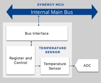
Temperature Sensor
Predicts and monitors the die temperature for reliable operation of the device.
The on-chip temperature sensor outputs a voltage inversely proportional to the die temperature, and the relationship between the die temperature and the output voltage is relatively linear. The output voltage is provided to the ADC for conversion and further use by the end-application.
A temperature sensor is available on the following Synergy MCUs.
S1 Series (Low Power): S124, S128, S1JA
S3 Series (High Efficiency): S3A1, S3A3, S3A6, S3A7
S5 Series (High Integration): S5D3, S5D5, S5D9
S7 Series (High Performance): S7G2
Timing & Control
Synergy MCUs feature a variety of timing and control functions necessary for real time applications.
The Asynchronous General Purpose Timer (AGT) provides timer functions and signal measurement and generation capabilities, while the general Pulse Width Modulation (PWM) timers generate pulse-based waveforms for a variety of applications. The Watchdog Timer (WDT) can be used to generate automatic MCU resets when unexpected program execution has occurred.
Asynchronous General Purpose Timer (AGT)
A 16-bit timer that provides a variety of signal measurement and generation capabilities, as well as counting functions.
AGT supports the following modes of operation:
- Timer mode
- Pulse output mode
- Event counter mode
- Pulse width measurement mode
- Pulse period measurement mode
AGT can be operated using several different clock sources such as a peripheral clock, a low-speed on-chip oscillator, and an underflow signal of the timer.
AGT is available on the following Synergy MCUs.
S1 Series (Low Power): S124, S128, S1JA
S3 Series (High Efficiency): S3A1, S3A3, S3A6, S3A7
S5 Series (High Integration): S5D3, S5D5, S5D9
S7 Series (High Performance): S7G2
General PWM Timer 16-Bit (GPT16)
A set of configurable 16-bit general purpose timers that can be used to generate PWM waveforms and perform pulse width measurements on input signals.
The PWM waveforms can be used for a variety of applications, including brushless DC motor control. Each GPT16 timer channel supports independent clock selection and can be triggered through internal events or external inputs. Timers can also interface with the Event Link Controller (ELC) and Data Transfer Controller (DTC) to synchronize with other system events.
GPT16 is available on the following Synergy MCUs.
S1 Series (Low Power): S124, S128, S1JA
S3 Series (High Efficiency): S3A1, S3A3, S3A6
General PWM Timer 32-Bit (GPT32)
A set of configurable 32-bit general purpose timers that can be used to generate PWM waveforms and perform pulse width measurements on input signals.
The PWM waveforms can be used for a variety of applications, including brushless DC motor control. Each GPT32 timer channel supports independent clock selection and can be triggered through internal events or external inputs. Timers can also interface with the Event Link Controller (ELC) and Data Transfer Controller (DTC) to synchronize with other system events.
GPT32 is available on the following Synergy MCUs.
S1 Series (Low Power): S124, S128, S1JA
S3 Series (High Efficiency): S3A1, S3A3, S3A6, S3A7
S5 Series (High Integration): S5D3, S5D5, S5D9
S7 Series (High Performance): S7G2
Watchdog Timer (WDT)
A 14-bit down counter that can be used to reset the MCU or generate a non-maskable interrupt when unexpected behavior occurs.
The WDT functions as a failsafe to return the MCU to a known state. It can be configured to start automatically or by writing to the counter register.
WDT is available on the following Synergy MCUs.
S1 Series (Low Power): S124, S128, S1JA
S3 Series (High Efficiency): S3A1, S3A3, S3A6, S3A7
S5 Series (High Integration): S5D3, S5D5, S5D9
S7 Series (High Performance): S7G2
Human Machine Interface (HMI)
Synergy MCUs provide a variety of HMI features for building interactive applications.
Several components offer hardware acceleration for user displays, while a touch sense input module enables capturing user actions. Some MCU groups also offer support for capturing parallel data from imaging and other external I/O devices.
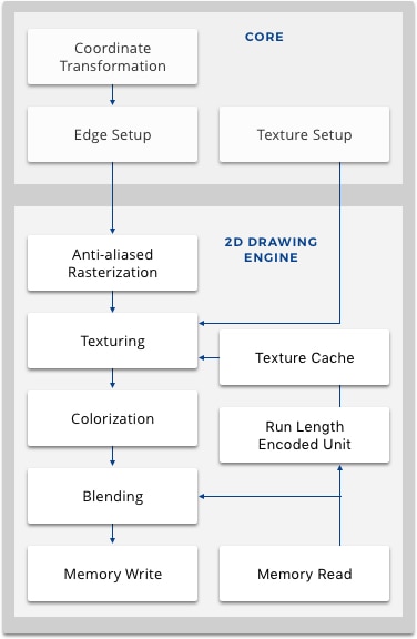
2D Drawing Engine (DRW)
Offloads the CPU by independently transferring graphical content to the frame buffer.
The DRW supports a variety of 2D graphic primitives such as lines, polygons, circles, ellipses, and quadratic Bezier curves along with custom geometries. It can perform fill, copy, rotate, scale, color conversion, and bilinear filtering. The engine functionality also includes alpha-blending, anti-aliasing, outlining, texture mapping, and transformation. The DRW supports Bit Boundary Block Transfer (BitBLT), which allows two bitmaps to be combined.
DRW is available on the following Synergy MCUs.
S5 Series (High Integration): S5D9
S7 Series (High Performance): S7G2
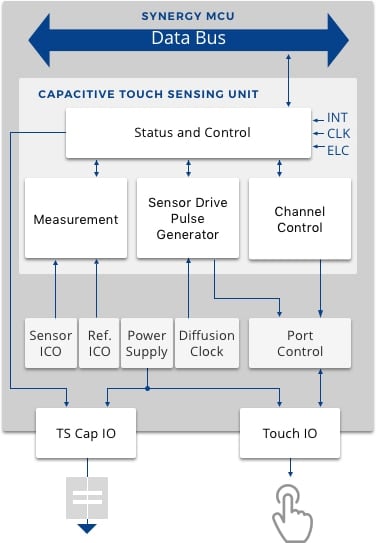
Capacitive Touch Sensing Unit (CTSU)
Enables detection for touch interfaces by measuring the change in capacitance of sensing electrodes.
The CTSU measures capacitance using either the self-capacitance method or mutual-capacitance method. With the self-capacitance method, the CTSU measures the capacitance between a finger and electrode, while the mutual-capacitance method measures the change in capacitance between two electrodes when a finger is present. CTSU measurement can be triggered by software or the ELC.
CTSU is available on the following Synergy MCUs.
S1 Series (Low Power): S124, S128, S1JA
S3 Series (High Efficiency): S3A1, S3A3, S3A6, S3A7
S5 Series (High Integration): S5D3, S5D5, S5D9
S7 Series (High Performance): S7G2
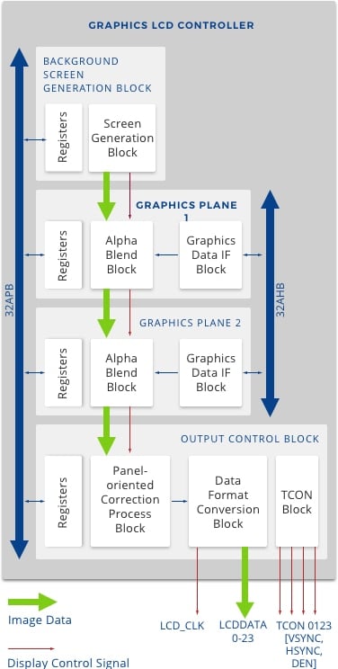
Graphics LCD Controller (GLCDC)
Drives a variety of color TFT LCD screens using the standard RGB and control signals.
The GLCDC outputs image data in either serial or parallel format, up to 24 bits. It can be used to superimpose two drawing planes and one background plane, and to perform enhancements such as alpha-blending, dither correction, brightness and contrast correction, and gamma correction. Low current consumption makes this controller suitable for handheld and battery-operated commercial and home applications.
GLCDC is available on the following Synergy MCUs.
S5 Series (High Integration): S5D9
S7 Series (High Performance): S7G2
JPEG Codec
Performs high-speed compression and decoding of JPEG image data.
The JPEG Codec engine supports multiple pixel formats for compression and decompression, and provides four Huffman tables for error management during decompression. The JPEG engine conforms to the JPEG baseline compression and decompression standard, JPEG Part 2, ISO-IEC 10918-2.
JPEG Codec is available on the following Synergy MCUs.
S5 Series (High Integration): S5D9
S7 Series (High Performance): S7G2
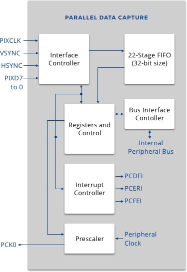
Parallel Data Capture Unit (PDC)
Transfers data from external peripherals such as cameras, scanners and other I/O devices, to on-chip SRAM or external memory.
The PDC configures transfers to be handled by either the DMA controller or Data Transfer Controller, and can capture up to 4095 lines of data in both vertical and horizontal directions. It supports detection of VSYNC and HSYNC video synchronization signals, and an external data transfer clock up to 30MHz.
PDC is available on the following Synergy MCUs.
S5 Series (High Integration): S5D9
S7 Series (High Performance): S7G2
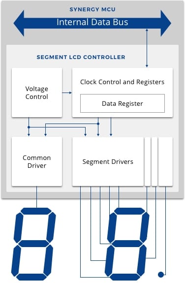
Segment LCD Controller (SLCDC)
Drives a variety of static LCD screens. Automatically generates segment and common signals based on the contents of the display data register.
The SLCDC can generate the LCD driver voltage from one of three sources:
- Internal voltage boost circuit
- Capacitor split circuit
- External resistor divider
When the internal voltage boost circuit is selected, the SLCDC can select between 16 steps of contrast adjustment by varying the LCD reference voltage.
SLCDC is available on the following Synergy MCUs.
S3 Series (High Efficiency): S3A1, S3A3, S3A6, S3A7
Connectivity
Synergy MCUs provide a wide range of options for connecting and communicating with external devices.
Several peripherals offer synchronous or asynchronous serial communications, such as Inter-Integrated Circuit (I2C), Serial Peripheral Interface (SPI), Serial Sound Interface (SSI), and the Serial Communications Interface (SCI). Also included are integrated USB and Ethernet controllers, providing high-performance communications for a variety of devices.
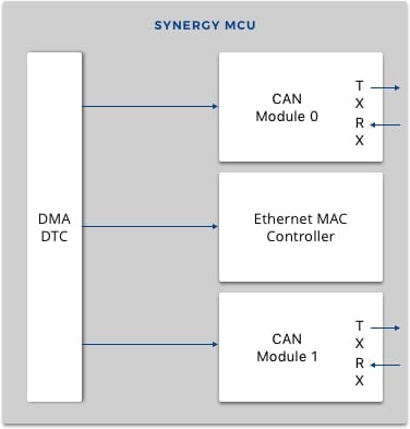
Controller Area Network (CAN)
Provides functionality to receive and transmit data using a message-based protocol between multiple slaves and masters in electromagnetically noisy applications.
The CAN interface complies with the ISO 11898-1 (CAN2.0A/CAN2.0B) standard and supports up to 32 mailboxes when configured in normal mailbox mode, or 24 mailboxes when operating in FIFO mode. Both standard (11-bit) and extended (29-bit) messaging formats are supported.
CAN is available on the following Synergy MCUs.
S1 Series (Low Power): S124, S128, S1JA
S3 Series (High Efficiency): S3A1, S3A3, S3A6, S3A7
S5 Series (High Integration): S5D3, S5D5, S5D9
S7 Series (High Performance): S7G2
Inter-Integrated Circuit Interface (I2C)
Provides asynchronous serial communication through a two-wire bus, supporting operation in I2C or System Management Bus (SMBus) mode.
The I2C interface can be configured in single-master, multi-master or slave mode, and allows for flexible slave address detection, including device ID, SMBus host and general call addresses. Fast Mode Plus, enabling data transmission speeds of up to 1Mbps, is available on select MCU series. The I2C module also includes a bus hanging timeout feature, which can act as a safeguard when the slave holds the clock low longer than expected.
I2C is available on the following Synergy MCUs.
S1 Series (Low Power): S124, S128, S1JA
S3 Series (High Efficiency): S3A1, S3A3, S3A6, S3A7
S5 Series (High Integration): S5D3, S5D5, S5D9
S7 Series (High Performance): S7G2
Infrared Data (IrDA) Interface
IrDA 1.0-compliant interface enables wireless communication for the Serial Communications Interface (SCI).
The IrDA transmit and receive pins are multiplexed with SCI transmit and receive pins. IrDA data transfer rates are configurable via software, from 9600bps up to 115200bps.
IrDA interface is available on the following Synergy MCUs.
S3 Series (High Efficiency): S3A3, S3A7
S5 Series (High Integration): S5D3, S5D5, S5D9
S7 Series (High Performance): S7G2
Quad Serial Peripheral Interface (QSPI)
Supports 4-bit multiplexed serial communication for ROM devices, providing up to four times the typical SPI bandwidth.
The QSPI module supports the following SPI protocols:
- SPI
- Extended SPI
- Dual SPI
- Quad SPI
The QSPI supports a timing adjustment feature and configurable address width, from 8 to 32 bits, enabling support for a wide range of flash devices. The QSPI also supports automatic generation of Read and Fast Read instructions to enable faster access to external ROMs.
QSPI is available on the following Synergy MCUs.
S3 Series (High Efficiency): S3A1, S3A3, S3A6, S3A7
S5 Series (High Integration): S5D3, S5D5, S5D9
S7 Series (High Performance): S7G2
Sampling Rate Converter (SRC)
Converts the sampling rate of data produced by various audio decoders such as WMA, MP3, and AAC, for both monaural and 16-bit stereo data.
The SRC contains independent FIFOs for input and output. In a typical application, a DMA controller can be used to transfer PCM audio data from RAM to the SRC. After sample rate conversion, the audio data can be transferred to the SSI, where it can be transmitted to an external audio codec.
SRC interface is available on the following Synergy MCUs.
S5 Series (High Integration): S5D3, S5D5, S5D9
S7 Series (High Performance): S7G2
SD/MMC Host Interface (SDHI)
Connects a variety of external memory cards, supporting both 1-bit and 4-bit buses for SD, SDHC, SDXC, as well as wireless network modules like Wi-Fi/BLE.
The MMC interface supports 1-, 4-, and 8-bit buses providing eMMC 4.51 device access.
SDHI is available on the following Synergy MCUs.
S3 Series (High Efficiency): S3A1, S3A3, S3A6
S5 Series (High Integration): S5D3, S5D5, S5D9
S7 Series (High Performance): S7G2
Serial Communications Interface (SCI)
Serial interface for external devices supporting the following modes of operation:
- Asynchronous (UART, ACIA)
- Synchronous interface (8-bit data length only)
- Simple I2C (master only) and Simple SPI (master only)
- Smart card interface
The smart card interface complies with the ISO/IEC 7816-3 standard for electronic signals and transmission protocol. An on-chip baud rate generator allows for configuring the data transfer speed.
SCI is available on the following Synergy MCUs.
S1 Series (Low Power): S124, S128, S1JA
S3 Series (High Efficiency): S3A1, S3A3, S3A6, S3A7
S5 Series (High Integration): S5D3, S5D5, S5D9
S7 Series (High Performance): S7G2
Serial Peripheral Interface (SPI)
Provides synchronous serial connectivity for full-duplex communication.
The SPI module can be configured for operation in multi-master, single-master or slave mode. In addition to normal SPI modes, the module can be configured for 3-wire clock synchronous operation, as well as transmit-only and loopback modes. The SPI module supports data rates of up to 30Mbps, and can detect underrun, overrun, parity, and mode fault errors.
SPI is available on the following Synergy MCUs.
S1 Series (Low Power): S124, S128, S1JA
S3 Series (High Efficiency): S3A1, S3A3, S3A6, S3A7
S5 Series (High Integration): S5D3, S5D5, S5D9
S7 Series (High Performance): S7G2
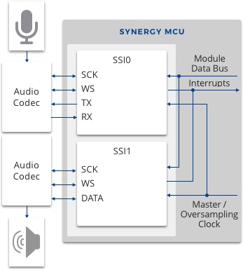
Serial Sound Interface (SSI)
Enables transmitting PCM audio data to digital audio devices.
The SSI supports an audio clock frequency of up to 50MHz, and can be configured as either a master or slave. In addition, the SSI can be configured as a transmitter, receiver or transceiver, depending on the needs of the application. The SSI includes 8-stage FIFO buffers in the receiver and transmitter. It supports interrupt and DMA-driven data reception and transmission.
SSI is available on the following Synergy MCUs.
S3 Series (High Efficiency): S3A1, S3A3, S3A6, S3A7
S5 Series (High Integration): S5D3, S5D5, S5D9
S7 Series (High Performance): S7G2
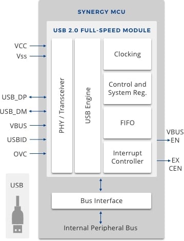
USB 2.0 Full-Speed Interface (USBFS)
Offers USB connectivity with operation in host, device, and On-The-Go (OTG) modes.
Host mode supports both full-speed and low-speed operation, while device mode supports full-speed operation only. Performs data transfer speeds of up to 12Mbps and is compliant with Battery Charging Class Specification Rev. 1.2. Synergy S1 Series MCUs support up to 5 pipes in internal buffer memory for assigning end points, while S3, S5 and S7 support up to 10 pipes. In addition, the module supports programmable intervals for isochronous and interrupt transfers when operating in host mode. Internal pull-up and pull-down resistors for D+ and D- signals and crystal-less operation simplify board designs and reduce overall system cost.
USBFS is available on the following Synergy MCUs.
S1 Series (Low Power): S124, S128, S1JA
S3 Series (High Efficiency): S3A1, S3A3, S3A6, S3A7
S5 Series (High Integration): S5D3, S5D5, S5D9
S7 Series (High Performance): S7G2
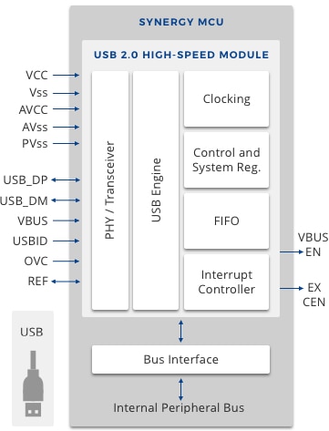
USB 2.0 High-Speed Interface (USBHS)
Offers USB connectivity with operation in host, device and On-The-Go (OTG) modes, including support for high-speed operation.
The USBHS supports data transfer speeds of up to 480Mbps and features both self-powered and bus-powered operation. The USBHS provides up to 10 pipes in internal buffer memory for assigning end points. When operating in host mode, the USBHS supports programmable intervals for isochronous and interrupt transfers, and automatically schedules Start of Frame (SOF) and packet transmissions. Internal pull-up and pull-down resistors for D+ and D- signals simplify board designs and reduce overall system cost.
USBHS is available on the following Synergy MCUs.
S5 Series (High Integration): S5D9
S7 Series (High Performance): S7G2
System Management
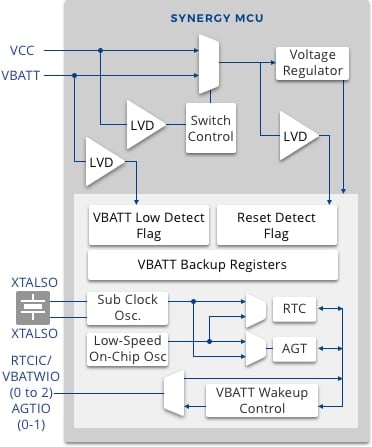
Battery Backup
Provides backup power in case of loss of VCC power.
The system monitors the VCC power supply voltage and switches to VBATT battery power when VCC drops below a threshold. The battery backup provides power for multiple modules, including the RTC, AGT, low-speed on-chip oscillator, and sub-clock oscillator. In addition, some Synergy MCUs support wakeup control functionality using external pins in VBATT mode.
Battery Backup is available on the following Synergy MCUs.
S3 Series (High Efficiency): S3A1, S3A3, S3A6, S3A7
S5 Series (High Integration): S5D3, S5D5, S5D9
S7 Series (High Performance): S7G2
Clock Management
Synergy MCUs can be operated from multiple clock sources, enabling flexible operation and optimization across several power and performance points.
The system clock can be provided externally, from a single-ended clock source, or can be generated internally using on-chip oscillators such as the main clock oscillator or sub-clock oscillator. Additionally, a dedicated on-chip 15kHz oscillator is used to operate an independent 14-bit watchdog timer.
Clock Management is available on the following Synergy MCUs.
S1 Series (Low Power): S124, S128, S1JA
S3 Series (High Efficiency): S3A1, S3A3, S3A6, S3A7
S5 Series (High Integration): S5D3, S5D5, S5D9
S7 Series (High Performance): S7G2
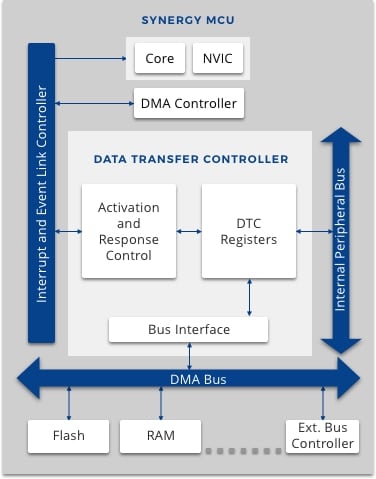
Data Transfer Controller (DTC)
Performs data transfers when activated by an interrupt request, without requiring CPU intervention.
The DTC supports the following modes of operation: normal transfer mode, repeat transfer mode and block transfer mode. The data transfer unit size can be 1 byte (8 bits), 1 word (16 bits), or 1 long word (32 bits), and a single block of data can consist of up to 256 units.
DTC is available on the following Synergy MCUs.
S1 Series (Low Power): S124, S128, S1JA
S3 Series (High Efficiency): S3A1, S3A3, S3A6, S3A7
S5 Series (High Integration): S5D3, S5D5, S5D9
S7 Series (High Performance): S7G2
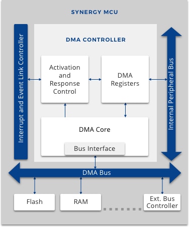
DMA Controller (DMAC)
Transfers data between memory and peripherals, or between two peripherals, without CPU intervention.
The DMAC supports multiple data transfer channels, each with its own priority, and can transfer up to 64MB of data. The DMAC supports the following modes of operation: normal transfer mode, repeat transfer mode and block transfer mode. The data transfer unit size can be 1 byte (8 bits), 1 word (16 bits), or 1 long word (32 bits), and a single block of data can consist of up to 1024 units. The DMAC supports multiple interrupt outputs to the CPU or DTC upon transfer completion.
DMAC is available on the following Synergy MCUs.
S3 Series (High Efficiency): S3A1, S3A3, S3A6, S3A7
S5 Series (High Integration): S5D3, S5D5, S5D9
S7 Series (High Performance): S7G2
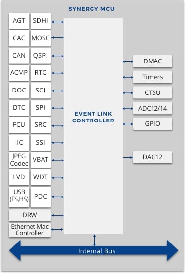
Event Link Controller (ELC)
Enables direct interaction between peripherals without CPU interaction, allowing for synchronization of system events.
Using the ELC, peripherals communicate via event signals that can be used to trigger actions such as:
The SLCDC can generate the LCD driver voltage from one of three sources:
- Start/Stop/Clear timer
- Capacitor split circuit
- Start ADC or DAC conversion
- Start capacitive touch measurement
- Start DMA/DTC transfer
- Issue interrupts to CPU
- Change state of GPIO pins
Using events enhances the ability to handle many events with a limited number of interrupt vectors.
ELC is available on the following Synergy MCUs.
S1 Series (Low Power): S124, S128, S1JA
S3 Series (High Efficiency): S3A1, S3A3, S3A6, S3A7
S5 Series (High Integration): S5D3, S5D5, S5D9
S7 Series (High Performance): S7G2
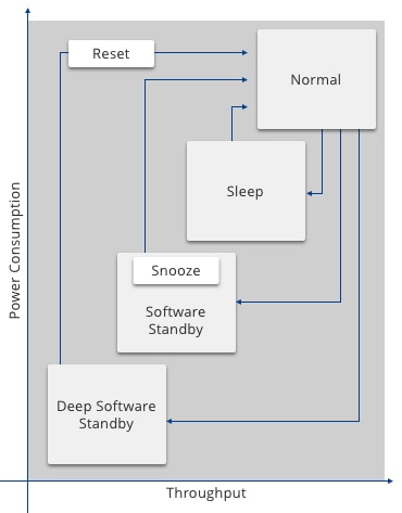
Low Power Modes
Provides flexible options for disabling or powering down selected MCU components, giving the user advanced control over MCU power consumption.
The system can put the CPU into clock-gated mode, and peripherals can be disabled or put into data retention mode for additional power savings. The system also provides independent wake-up signals for data acquisition and data transmission peripherals.
Low Power Modes are available on the following Synergy MCUs.
S1 Series (Low Power): S124, S128, S1JA
S3 Series (High Efficiency): S3A1, S3A3, S3A6, S3A7
S5 Series (High Integration): S5D3, S5D5, S5D9
S7 Series (High Performance): S7G2
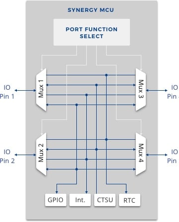
Port Function Select (PFS)
Synergy MCUs offer flexibility in pin configuration, allowing the user to map peripheral signals to different external pins as needed.
Pins can be configured for port direction, internal pull-up control, drive strength, edge detection, and other parameters. The PFS simplifies printed circuit board layout and routing, and enables easier migration between Synergy MCUs.
PFS is available on the following Synergy MCUs.
S1 Series (Low Power): S124, S128, S1JA
S3 Series (High Efficiency): S3A1, S3A3, S3A6, S3A7
S5 Series (High Integration): S5D3, S5D5, S5D9
S7 Series (High Performance): S7G2
Real-Time Clock (RTC)
Provides standard clock and calendar functionality, and functions as a configurable interrupt source.
The RTC includes support for both Western and non-Western calendars. Interrupts can be triggered based on a specific date and time, on a periodic basis, or based on specific events. The RTC can also be used to send event signals to peripherals and to wake the CPU from Sleep or Software Standby mode.
RTC is available on the following Synergy MCUs.
S1 Series (Low Power): S124, S128, S1JA
S3 Series (High Efficiency): S3A1, S3A3, S3A6, S3A7
S5 Series (High Integration): S5D3, S5D5, S5D9
S7 Series (High Performance): S7G2
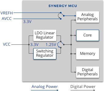
Switching Regulator
The low-power switching regulator and a low-dropout (LDO) voltage regulator supply power to the core, memory subsystem and other digital peripherals.
The internal power rail for these components can be switched to either source depending on application requirements. The switching regulator is a low-quiescent DC/DC buck converter that reduces power consumption and increases efficiency for high-load currents.
A switching regulator is available on the high performance Synergy S7G2 MCUs.
SysTick
A 24-bit down counter that can be used as an RTOS system heartbeat, a task-scheduler, an interrupt source, or for application-specific usage.
SysTick can be clocked by the Low-speed On-chip Oscillator (LOCO).
SysTick is available on the following Synergy MCUs.
S1 Series (Low Power): S124, S128, S1JA
S3 Series (High Efficiency): S3A1, S3A3, S3A6, S3A7
S5 Series (High Integration): S5D3, S5D5, S5D9
S7 Series (High Performance): S7G2
Safety
ADC Diagnostics
The ADC modules feature integrated diagnostic capabilities to detect improper ADC behavior and loss of external signal connection at input pins.
To ensure proper functionality of the ADC, the system performs a diagnostic check before each scan using a pre-determined test voltage. Additionally, the system includes a built-in charging/discharging circuit for input pins that enables reliable detection of input signal disconnect and prevents erroneous readings.
ADC Diagnostics is available on the following Synergy MCUs.
S1 Series (Low Power): S124, S128, S1JA
S3 Series (High Efficiency): S3A1, S3A3, S3A6, S3A7
S5 Series (High Integration): S5D3, S5D5, S5D9
S7 Series (High Performance): S7G2
Clock Frequency Accuracy Measurement Circuit (CAC)
Provides clock measurement and testing capabilities to ensure accurate frequency on internal system clocks.
The CAC tests for frequency accuracy by comparing the target clock with a reference clock, which can be specified as either an internal oscillator or an external clock source. The CAC is suitable for meeting requirements of the IEC 60730 Safety Standard for Household Appliances.
CAC is available on the following Synergy MCUs.
S1 Series (Low Power): S124, S128, S1JA
S3 Series (High Efficiency): S3A1, S3A3, S3A6, S3A7
S5 Series (High Integration): S5D3, S5D5, S5D9
S7 Series (High Performance): S7G2
Cyclic Redundancy Check (CRC) Calculator
Generates CRC codes to detect errors on CPU data reads and writes.
The CRC includes a snoop feature that can be configured to monitor reads to and writes from specific addresses for automatic CRC generation. Several polynomials are available for CRC generation.
CRC is available on the following Synergy MCUs.
S1 Series (Low Power): S124, S128, S1JA
S3 Series (High Efficiency): S3A1, S3A3, S3A6, S3A7
S5 Series (High Integration): S5D3, S5D5, S5D9
S7 Series (High Performance): S7G2
Data Operation Circuit (DOC)
Performs 16-bit addition, subtraction and comparison without CPU intervention. This is useful for background run-time tests of data integrity in SRAM.
The DOC can be configured to trigger an interrupt or ELC event as a result of the comparison, and is useful in reducing CPU load while performing tests on large sections of memory. The DOC is suitable for meeting requirements of the IEC 60730 Safety Standard for Household Appliances.
DOC is available on the following Synergy MCUs.
S1 Series (Low Power): S124, S128, S1JA
S3 Series (High Efficiency): S3A1, S3A3, S3A6, S3A7
S5 Series (High Integration): S5D3, S5D5, S5D9
S7 Series (High Performance): S7G2
Error Correction Code (ECC) in SRAM
Detects and corrects errors in real-time in specific regions of on-chip SRAM called ECCRAM.
The built-in ECC functionality detects 1- or 2-bit errors, and automatically corrects 1-bit errors. It can be enabled or disabled, and can be configured to trigger interrupts upon error detection.
ECC is available on the following Synergy MCUs.
S1 Series (Low Power): S124, S128, S1JA
S3 Series (High Efficiency): S3A1, S3A3, S3A6, S3A7
S5 Series (High Integration): S5D3, S5D5, S5D9
Flash Area Protection
Provides a safety mechanism to write-protect an area of code flash during self-programming.
This feature protects against accidental corruption of memory needed to maintain system functionality, and is suitable for meeting requirements of the IEC 60730 Safety Standard for Household Appliances.
Flash Area Protection is available on the following Synergy MCUs.
S1 Series (Low Power): S124, S128, S1JA
S3 Series (High Efficiency): S3A1, S3A3, S3A6, S3A7
S5 Series (High Integration): S5D3, S5D5, S5D9
S7 Series (High Performance): S7G2
Independent Watchdog Timer (IWDT)
Provides a failsafe mechanism to reset the MCU or generate a non-maskable interrupt when system operation is unstable.
The IWDT consists of a 14-bit down counter and can be triggered on an underflow or refresh error. The timer operates independently on a dedicated clock source.
IWDT is available on the following Synergy MCUs.
S1 Series (Low Power): S124, S128, S1JA
S3 Series (High Efficiency): S3A1, S3A3, S3A6, S3A7
S5 Series (High Integration): S5D3, S5D5, S5D9
S7 Series (High Performance): S7G2
Port Output Enable Module for GPT (POEG)
Provides a safety mechanism to disable General PWM Timer (GPT) output pins in case of an emergency.
The POEG can be triggered via the following sources:
- External signal input
- Comparator interrupt
- Timer error
- Oscillation stop detection
- Software control
POEG is available on the following Synergy MCUs.
S1 Series (Low Power): S124, S128, S1JA
S3 Series (High Efficiency): S3A1, S3A3, S3A6, S3A7
S5 Series (High Integration): S5D3, S5D5, S5D9
S7 Series (High Performance): S7G2
SRAM Parity Error Check
Detects memory errors and triggers an interrupt or system reset.
The system appends a parity bit to 8-bit words written to SRAM, and performs a parity check when reading from SRAM. Parity checking is performed on all sections of SRAM except ECCRAM. This feature is suitable for meeting requirements of the IEC 60730 Safety Standard for Household Appliances.
SRAM Parity Error Check is available on the following Synergy MCUs.
S1 Series (Low Power): S124, S128, S1JA
S3 Series (High Efficiency): S3A1, S3A3, S3A6, S3A7
S5 Series (High Integration): S5D3, S5D5, S5D9
S7 Series (High Performance): S7G2
Security & Encryption
Synergy MCUs feature a range of security and encryption features to enable secure data communications and storage.
These features leverage a variety of National Institute of Standards and Technology (NIST)-compliant cryptographic algorithms, such as the Advanced Encryption Standard (AES) 128/256 protocol. Security features also include true random number generation to create secure cryptographic keys, and hash generation functions to ensure data integrity.
Secure Crypto Engine 7 (SCE7)
Facilitates secure data communications and storage to protect sensitive or confidential data.
The SCE7 module implements security and encryption functions, leveraging a variety of NIST-compliant cryptographic algorithms. The SCE7 module includes a 128-bit true random number generator (TRNG), and supports many symmetric and asymmetric algorithms, including:
- AES 128/192/256
- 3DES
- ARC4
- DSA 1024/2048
- RSA
In addition, SCE7 also generates hash values to ensure data integrity. The module supports the following functions:
- SHA1/224/256
- GHASH
SCE7 is available on the following Synergy MCUs.
S5 Series (High Integration): S5D3, S5D5, S5D9
S7 Series (High Performance): S7G2
Secure Crypto Engine 5 (SCE5)
Facilitates secure data communications and storage to protect sensitive or confidential data.
The SCE5 module implements security and encryption functions, leveraging a variety of NIST-compliant cryptographic algorithms. The SCE5 module includes a 128-bit true random number generator (TRNG) and supports the AES 128/256 encryption protocol. In addition, the module can generate hash values to ensure data integrity.
SCE5 is available on the high efficiency Synergy S3A1, S3A3, S3A6, and S3A7 MCUs.
AES (128/256) & TRNG
A built-in, 128-bit true random number generator (TRNG) uses internal noise to generate cryptographically secure random numbers, and the Advanced Encryption Standard (AES) 128/256 protocols offload software and save power for encryption and decryption of data.
AES (128/256) and TRNG are available on the low power Synergy S124, S128 and S1JA MCUs.
Support

Support Communities


