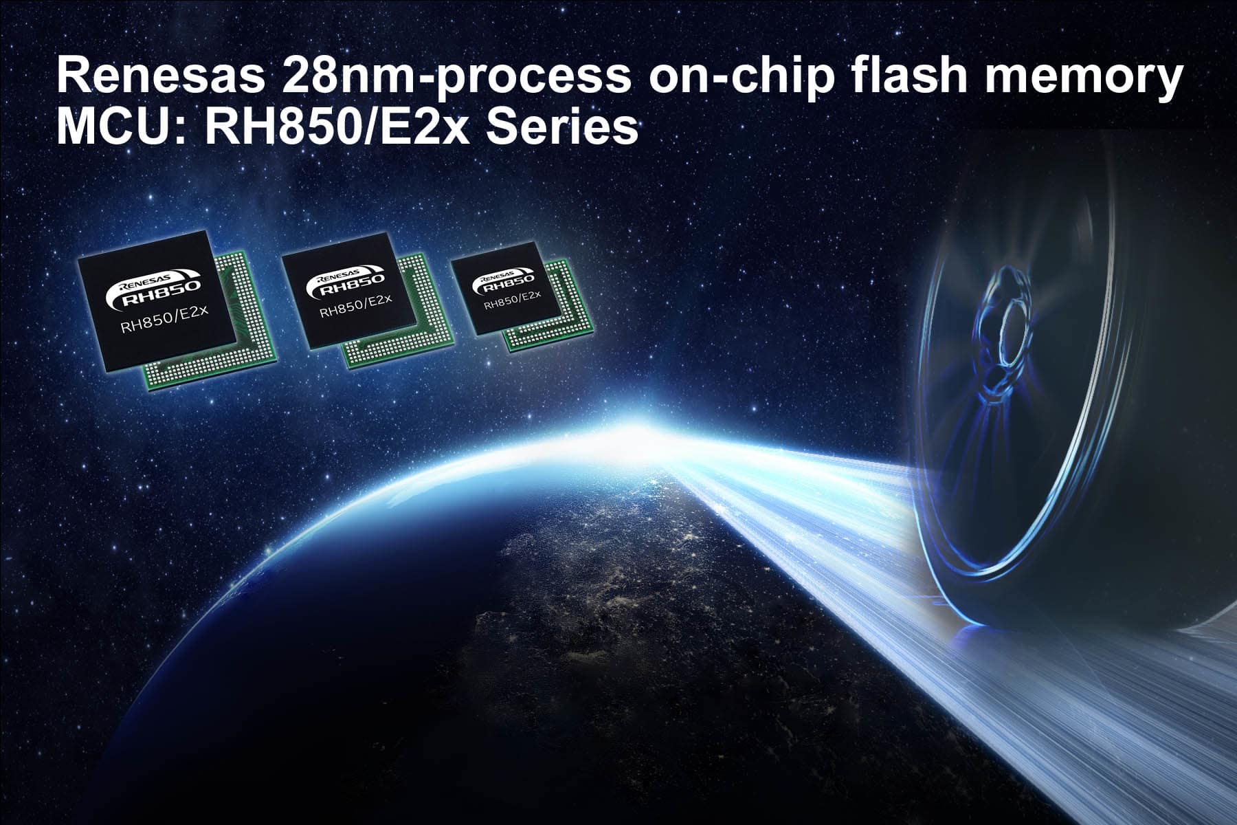
TOKYO, Japan, March 27, 2018 — Renesas Electronics Corporation (TSE: 6723), a premier supplier of advanced semiconductor solutions, today announced the sample shipment of the industry's first on-chip flash memory microcontroller (MCU) using a 28 nanometer (nm) process technology. To contribute to the realization of next-generation green cars and autonomous vehicles with higher efficiency and higher reliability, the revolutionary RH850/E2x Series MCU incorporates up to six 400 megahertz (MHz) CPU cores, which makes it the first on-chip flash memory automotive MCU to achieve the industry's highest processing performance (Note 1) of 9600 MIPS (Note 2). The new MCU series also features a built-in flash memory of up to 16 megabytes (MB) as well as enhanced security functions and functional safety.
Under Renesas autonomy™, an open, innovative and trusted platform for assisted and automated driving, Renesas provides end-to-end solutions that advance the evolution of vehicles towards next-generation green cars, connected cars, and autonomous-driving vehicles. The 28nm-generation automotive control MCU is a new breakthrough product featuring next-generation technology for achieving vehicle control, which, together with the R-Car Family of systems-on-chip (SoCs) designed for cloud connectivity and sensing, constitute the two main pillars of the Renesas autonomy Platform. Car OEMs and Tier 1 manufacturers, such as Denso Corporation, have already started to adopt the new 28nm MCU, recognizing the MCU’s superior processing performance capable of developing next-generation fuel-efficient engines, as well as its unparalleled scalability as a platform that addresses the expected electronic control unit (ECU) integration to come from changes in automotive electrics/electronics (E/E) architecture.
Key features of the new RH850/E2x MCU Series
High processing performance to enable complex automotive control for green cars
To develop environmentally-friendly vehicles, next-generation fuel-efficient engines require high processing performance to allow the implementation of new fuel combustion systems. In addition, both high processing performance and high integration densities are required to achieve miniaturization and higher efficiency in the motors and inverters used in electric vehicles (EV) and plug-in hybrid electric vehicles (PHEV). The newly-developed 28nm-process flash memory MCU is the world’s first to achieve up to six 400 MHz CPU cores and 9600 MIPS processing capabilities. Compared to the earlier 40nm MCUs, the new RH850/E2x Series of MCUs also achieves approximately three times the performance at the same power level. The RH850/E2x realizes increased automotive control system integration by including enhanced sensor interfaces necessary for precise automotive control functions. Multi-core virtual environments and model-based development environments for the new MCUs will be available from Renesas partner companies.
Advanced OTA updates with large flash memory capacities for connected cars
Demand for built-in large capacity flash memory is rising to support over-the-air (OTA) functionality which automatically and wirelessly updates the ECU software to control programs with improved safety. The RH850/E2x Series is equipped with up to 16 MB of flash ROM and, to suit the user’s needs and preferences, it is possible to only update certain arbitrary areas during program operation. The RH850/E2x Series also comes with improved serial interfaces, including up to ten channels of CAN FD and one Ethernet channel. Security functions that support Evita Medium enable the MCUs to support safe and rapid OTA updating of the software.
Enhanced functional safety for autonomous-driving vehicles
Targeting ASIL-D, the highest level of the ISO 26262 functional safety standard for automotive E/E systems, the RH850/E2x Series adopts the dual core lock step CPU structure that guarantees that the calculations performed by two CPU cores are identical. The RH850/E2x also provides up to four sets of CPU pairs, and features a variety of hardware functional safety improvements. In applications where a system malfunction could lead to life-endangering accidents, these features immediately detect faults should a malfunction occur and allow system safety to be maintained. Renesas will provide safety analysis tools that can flexibly support a wide range of use cases to implement safe systems.
Following the development of the 28nm embedded flash memory in February 2015, Renesas announced its collaboration with TSMC on 28nm MCUs in September 2016. The company today hit a major milestone by reaching sample shipment of the world’s first 28nm embedded flash memory MCU on the market. Renesas has already succeeded in verifying large-scale operation of fin-structure MONOS flash memory targeting 16/14nm and beyond generations of MCUs. As the leading supplier of automotive semiconductor solutions, Renesas is committed to advancing the industry through continued technological innovation to achieve a safe and secure automotive society.
To assure scalability in the RH850/E2x Series, in addition to the 28nm flash memory MCU, Renesas has also launched a 40nm process MCU featuring (1) and (3) described above. Samples of this MCU are available now. Samples of both 28nm and 40nm MCUs from RH850/E2x are scheduled to be available from March 2018.
Refer to the separate sheet (PDF: 74 KB) for product specifications of the RH850/E2x Series.
For more solution information, please visit https://www.renesas.com/en/solutions/automotive/powertrain.html
(Note 1) As of today compared to published data from other companies, according to Renesas research.
(Note 2) MIPS (Million Instructions Per Second): An expression of the processing power of a computer.
About Renesas’ Metal-Oxide-Nitride-Oxide-Silicon (MONOS) embedded flash technology
MONOS is a structure in which each transistor in the flash cell consists of three layers—oxide, nitride, and oxide—on a silicon base, with a metal control gate at the top. Renesas has accumulated more than two decades of experience in the use of MONOS flash memory technology by providing MCUs for IC cards. Based on the track record in MONOS technology, Renesas successfully extended the technology by developing a split-gate (SG) structure suitable for MCU internal flash memory. The new “SG-MONOS” –type flash memory realizes MCUs with high reliability, high speed and low power consumption.
About Renesas Electronics Corporation
Renesas Electronics Corporation (TSE: 6723) delivers trusted embedded design innovation with complete semiconductor solutions that enable billions of connected, intelligent devices to enhance the way people work and live. A global leader in microcontrollers, analog, power, and SoC products, Renesas provides comprehensive solutions for a broad range of automotive, industrial, infrastructure, and IoT applications that help shape a limitless future. Learn more at renesas.com. Follow us on LinkedIn, Facebook, Twitter, and YouTube.
(Remarks) Renesas autonomy is a trademark of Renesas Electronics Corporation. All registered trademarks or trademarks are the property of their respective owners.
The content in the press release, including, but not limited to, product prices and specifications, is based on the information as of the date indicated on the document, but may be subject to change without prior notice.