
Features
- Jitter below 100fs RMS maximum (10Hz to 20MHz)
- PLL core consists of fractional-feedback Analog PLL (APLL)
- Operates from a 25MHz to 80MHz crystal or XO
- APLL frequency independent of input / crystal frequency
- Operates as a frequency synthesizer or Digitally Controlled Oscillator (DCO)
- DCO has tuning granularity of < 1ppb
- Programmable status output
- 4 differential / 8 LVCMOS outputs
- Any frequency from 10MHz to 1GHz (180MHz for LVCMOS)
- Programmable output buffer supports HCSL (DC-coupled), LVDS/LVPECL/CML (AC-coupled) or two LVCMOS
- Differential output swing is selectable: 400mV to 800mV
- Output clock phase individually adjustable in 100ps steps
- Output Enable input with programmable effect
- Supports up to 1MHz I2C or up to 20MHz SPI serial processor port
- Can configure itself automatically after reset via internal customer-definable One-Time Programmable (OTP) memory with up to four different configurations
- 4 × 4 mm 24-VFQFPN package
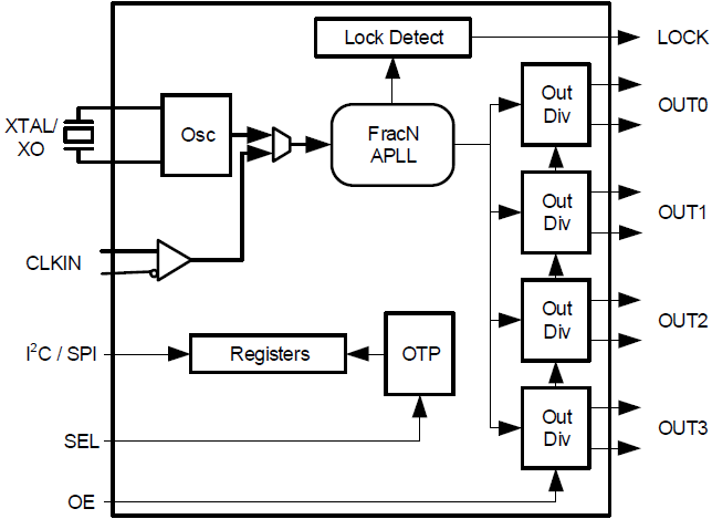
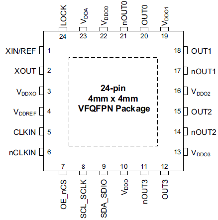

RC22504A - Block Diagram

Description
The RC22504A is a small, low-power timing component designed to be placed immediately adjacent to a PHY, switch, ASIC or FPGA that requires several reference clocks with jitter performance less than 100fs (max). The RC22504A can act as a frequency synthesizer to locally generate the reference clock or as a DCO for frequency margining or OTN clock applications.
This device is factory-configurable.
Try the Custom Part Configuration Utility.
Try the Custom Part Configuration Utility.
Parameters
| Attributes | Value |
|---|---|
| Diff. Outputs | 4 |
| Outputs (#) | 4 |
| Output Type | LVCMOS, HCSL, LVDS |
| Output Freq Range (MHz) | 10 - 1000 |
| Input Freq (MHz) | 25 - 312.5 |
| Inputs (#) | 2 |
| Input Type | Crystal, HCSL, LVDS, LVCMOS |
| Output Banks (#) | 4 |
| Core Voltage (V) | 1.8V, 3.3V |
| Output Voltage (V) | 1.8 |
| Feedback Input | No |
| Product Category | FemtoClock 2, Ultra-Low Jitter Clocks (<300 fs RMS), Extreme Performance Clocks (<150 fs RMS), Network Synchronization, PDH and SONET/SDH Clocks, Programmable Clocks |
Package Options
| Pkg. Type | Pkg. Dimensions (mm) | Lead Count (#) | Pitch (mm) |
|---|---|---|---|
| VFQFPN | 4.0 x 4.0 x 0.8 | 24 | 0.5 |
This device is factory-configurable.
Try the Custom Part Configuration Utility.
Try the Custom Part Configuration Utility.
| Part Number | Status | Samples | Longevity | Stock | Package | Budgetary Price (USD) | Lead Count (#) | Carrier Type | Moisture Sensitivity Level (MSL) | Qty. per Reel (#) | Qty. per Carrier (#) | Pb (Lead) Free | Pb Free Category | Temp. Range (°C) | Country of Assembly | Country of Wafer Fabrication |
|---|---|---|---|---|---|---|---|---|---|---|---|---|---|---|---|---|
| RC22504A000GNK#BB0 | Active | Available | 2040 Apr | Out of Stock | VFQFPN | 1ku | $6.49 | 24# | Tray | 1 | 0 | 490# | Yes | e3 Sn | -40 to 85°C | TAIWAN | SINGAPORE |
| RC22504A000GNK#KB0 | Active | N/A | 2040 Apr | Out of Stock | VFQFPN | 1ku | $6.49 | 24# | Reel | 1 | 2500# | 0 | Yes | e3 Sn | -40 to 85°C | TAIWAN | SINGAPORE |
Loading
Log in required to subscribe
- Application NotePDF 1.53 MB R31AN0034EU0102 Rev.1.02 Oct 21, 2025AI-generated Summary: PLL loop filter design involves selecting component values to ensure stable operation and optimized phase noise. The loop bandwidth depends on parameters like charge pump current, VCO gain, and feedback divider. Second and third order passive loop filters are common, with specific calculations for cutoff, zero, and pole frequencies guiding component selection. Proper tuning of loop bandwidth enhances PLL stability and phase noise performance, demonstrated through lab experiments and calculation examples.
- Manual - SoftwarePDF 2.21 MB R31US0012EU0102 Rev.1.02 May 23, 2024
- Application NotePDF 129 KB Aug 04, 2021AI-generated Summary: FemtoClock 2 enables precise frequency margining through I2C-controlled configuration of output clock frequencies. It uses a fractional-N APLL with a 27-bit feedback divider for fine frequency resolution and integer output dividers for individual outputs. Frequency changes can be made glitch-free by adjusting output dividers or more precisely by modifying the fractional feedback divider, which may require APLL recalibration if changes exceed ±0.1%. The document details register addressing, frequency adjustment methods, and calibration procedures to optimize clock output performance.
- Application NotePDF 256 KB Jul 05, 2021AI-generated Summary: The document explains methods to generate a 1.2V LVCMOS signal from a 1.8V LVCMOS output by attenuating the amplitude without lowering the driver voltage. It details typical LVCMOS driver and receiver configurations, impedance matching using source termination, and the use of a parallel resistor at the receiver input to reduce signal amplitude. Simulation and measurement results demonstrate that adding a parallel resistor effectively lowers the voltage to 1.2V while maintaining signal integrity and minimal impact on jitter and frequency. This approach supports flexible amplitude adjustment for various low-voltage LVCMOS requirements in clock signal applications.
- Application NotePDF 433 KB May 10, 2021AI-generated Summary: The FemtoClock2 Python driver enables users to create or load device setting files and program devices via USB-to-I2C adapters like Aardvark or FTDI. It requires Python 3.6.8 and provides a command line interface (CLI) for device configuration, connection, and I/O operations. Users can create synthesizer configurations using smart config commands, connect to devices, read/write data, and save settings. The driver supports scripting via Python, allowing programmatic device configuration and programming. Driver installation, update procedures, and command usage details are included.
- Application NotePDF 353 KB Mar 07, 2021AI-generated Summary: High bandwidth jitter attenuation uses the RC22504A and RC32504A synthesizers to reduce phase jitter caused by spurious noise above 1MHz offsets. The RC22504A operates with a high loop bandwidth (500kHz to 1MHz) and does not require a crystal, enabling a smaller, cost-effective solution. It supports flexible differential clock inputs compatible with various logic types. High bandwidth jitter attenuation is ideal for clock generators with multiple outputs and frequencies, such as Renesas’ ClockMatrix, improving phase jitter from around 150-200fs to below 100fs. Adjusting the APLL loop bandwidth optimizes filtering based on spur frequency. Measurement results demonstrate significant phase noise reduction and jitter improvement.
- Application NotePDF 170 KB 7WDXRDKU4E7E-5-57318 May 13, 2014
- Application NotePDF 495 KB 7WDXRDKU4E7E-5-57312 May 12, 2014
Recommended Documents (1)
Datasheets (1)
- Manual - SoftwarePDF 2.21 MB R31US0012EU0102 Rev.1.02 May 23, 2024
Manuals & Guides (3)
- Application NotePDF 1.53 MB R31AN0034EU0102 Rev.1.02 Oct 21, 2025AI-generated Summary: PLL loop filter design involves selecting component values to ensure stable operation and optimized phase noise. The loop bandwidth depends on parameters like charge pump current, VCO gain, and feedback divider. Second and third order passive loop filters are common, with specific calculations for cutoff, zero, and pole frequencies guiding component selection. Proper tuning of loop bandwidth enhances PLL stability and phase noise performance, demonstrated through lab experiments and calculation examples.
- Application NotePDF 1.99 MB 7WDXRDKU4E7E-5-57242 Mar 01, 2022
- Application NotePDF 129 KB Aug 04, 2021AI-generated Summary: FemtoClock 2 enables precise frequency margining through I2C-controlled configuration of output clock frequencies. It uses a fractional-N APLL with a 27-bit feedback divider for fine frequency resolution and integer output dividers for individual outputs. Frequency changes can be made glitch-free by adjusting output dividers or more precisely by modifying the fractional feedback divider, which may require APLL recalibration if changes exceed ±0.1%. The document details register addressing, frequency adjustment methods, and calibration procedures to optimize clock output performance.
- Application NotePDF 256 KB Jul 05, 2021AI-generated Summary: The document explains methods to generate a 1.2V LVCMOS signal from a 1.8V LVCMOS output by attenuating the amplitude without lowering the driver voltage. It details typical LVCMOS driver and receiver configurations, impedance matching using source termination, and the use of a parallel resistor at the receiver input to reduce signal amplitude. Simulation and measurement results demonstrate that adding a parallel resistor effectively lowers the voltage to 1.2V while maintaining signal integrity and minimal impact on jitter and frequency. This approach supports flexible amplitude adjustment for various low-voltage LVCMOS requirements in clock signal applications.View More (23)
Application Notes & White Papers (23)
No Results Found.
Check Spelling
Make sure all keywords are spelled correctly.
Make sure all keywords are spelled correctly.
Adjust Keywords
Try fewer, different, or more general terms to vary your search.
Try fewer, different, or more general terms to vary your search.
Review Filters
If you have filters applied, consider deselecting some to broaden your results.
If you have filters applied, consider deselecting some to broaden your results.
Need help?
- Search our extensive knowledgebase, designed to help customers with their FAQs.
- Get help from our expert Renesas technical staff and community on our support forums.
No Results Found.
Check Spelling
Make sure all keywords are spelled correctly.
Make sure all keywords are spelled correctly.
Adjust Keywords
Try fewer, different, or more general terms to vary your search.
Try fewer, different, or more general terms to vary your search.
Review Filters
If you have filters applied, consider deselecting some to broaden your results.
If you have filters applied, consider deselecting some to broaden your results.
Need help?
- Search our extensive knowledgebase, designed to help customers with their FAQs.
- Get help from our expert Renesas technical staff and community on our support forums.
No Results Found.
Check Spelling
Make sure all keywords are spelled correctly.
Make sure all keywords are spelled correctly.
Adjust Keywords
Try fewer, different, or more general terms to vary your search.
Try fewer, different, or more general terms to vary your search.
Review Filters
If you have filters applied, consider deselecting some to broaden your results.
If you have filters applied, consider deselecting some to broaden your results.
Need help?
- Search our extensive knowledgebase, designed to help customers with their FAQs.
- Get help from our expert Renesas technical staff and community on our support forums.
No Results Found.
Check Spelling
Make sure all keywords are spelled correctly.
Make sure all keywords are spelled correctly.
Adjust Keywords
Try fewer, different, or more general terms to vary your search.
Try fewer, different, or more general terms to vary your search.
Review Filters
If you have filters applied, consider deselecting some to broaden your results.
If you have filters applied, consider deselecting some to broaden your results.
Need help?
- Search our extensive knowledgebase, designed to help customers with their FAQs.
- Get help from our expert Renesas technical staff and community on our support forums.
No Results Found.
Check Spelling
Make sure all keywords are spelled correctly.
Make sure all keywords are spelled correctly.
Adjust Keywords
Try fewer, different, or more general terms to vary your search.
Try fewer, different, or more general terms to vary your search.
Review Filters
If you have filters applied, consider deselecting some to broaden your results.
If you have filters applied, consider deselecting some to broaden your results.
Need help?
- Search our extensive knowledgebase, designed to help customers with their FAQs.
- Get help from our expert Renesas technical staff and community on our support forums.
No Results Found.
Check Spelling
Make sure all keywords are spelled correctly.
Make sure all keywords are spelled correctly.
Adjust Keywords
Try fewer, different, or more general terms to vary your search.
Try fewer, different, or more general terms to vary your search.
Review Filters
If you have filters applied, consider deselecting some to broaden your results.
If you have filters applied, consider deselecting some to broaden your results.
Need help?
- Search our extensive knowledgebase, designed to help customers with their FAQs.
- Get help from our expert Renesas technical staff and community on our support forums.
No Results Found.
Check Spelling
Make sure all keywords are spelled correctly.
Make sure all keywords are spelled correctly.
Adjust Keywords
Try fewer, different, or more general terms to vary your search.
Try fewer, different, or more general terms to vary your search.
Review Filters
If you have filters applied, consider deselecting some to broaden your results.
If you have filters applied, consider deselecting some to broaden your results.
Need help?
- Search our extensive knowledgebase, designed to help customers with their FAQs.
- Get help from our expert Renesas technical staff and community on our support forums.
No Results Found.
Check Spelling
Make sure all keywords are spelled correctly.
Make sure all keywords are spelled correctly.
Adjust Keywords
Try fewer, different, or more general terms to vary your search.
Try fewer, different, or more general terms to vary your search.
Review Filters
If you have filters applied, consider deselecting some to broaden your results.
If you have filters applied, consider deselecting some to broaden your results.
Need help?
- Search our extensive knowledgebase, designed to help customers with their FAQs.
- Get help from our expert Renesas technical staff and community on our support forums.
Other (1)
No Results Found.
Check Spelling
Make sure all keywords are spelled correctly.
Make sure all keywords are spelled correctly.
Adjust Keywords
Try fewer, different, or more general terms to vary your search.
Try fewer, different, or more general terms to vary your search.
Review Filters
If you have filters applied, consider deselecting some to broaden your results.
If you have filters applied, consider deselecting some to broaden your results.
Need help?
- Search our extensive knowledgebase, designed to help customers with their FAQs.
- Get help from our expert Renesas technical staff and community on our support forums.
No Results Found.
Check Spelling
Make sure all keywords are spelled correctly.
Make sure all keywords are spelled correctly.
Adjust Keywords
Try fewer, different, or more general terms to vary your search.
Try fewer, different, or more general terms to vary your search.
Review Filters
If you have filters applied, consider deselecting some to broaden your results.
If you have filters applied, consider deselecting some to broaden your results.
Need help?
- Search our extensive knowledgebase, designed to help customers with their FAQs.
- Get help from our expert Renesas technical staff and community on our support forums.
Renesas Boards & Kits

RC32504A-EVK
Active
FemtoClock 2 Evaluation Kit
This is the evaluation kit for the RC32504A and RC22504A point-of-use jitter attenuator and clock generators. The board comes populated with an RC32504A device. The RC22504A is functionally a subset of the RC32504A, so this board can be used to evaluate either, or both, of the devices. Refer to... Read More
Recommended Documents:
Loading
Filters
Applied Filters
Software & Tools
Filter by Type
Filter by Provider
Sample Code
Filter by Application
Filter by Function
Filter by Compiler
Filter by IDE
Simulation Models
Partner Solutions
- Software PackageThe Renesas IC Toolbox (RICBox) software platform enables customers to configure Renesas devices on evaluation kits when attached to the computer running the software.
No Results Found.
Check Spelling
Make sure all keywords are spelled correctly.
Make sure all keywords are spelled correctly.
Adjust Keywords
Try fewer, different, or more general terms to vary your search.
Try fewer, different, or more general terms to vary your search.
Review Filters
If you have filters applied, consider deselecting some to broaden your results.
If you have filters applied, consider deselecting some to broaden your results.
Need help?
- Search our extensive knowledgebase, designed to help customers with their FAQs.
- Get help from our expert Renesas technical staff and community on our support forums.
- Software PackageThe Renesas IC Toolbox (RICBox) software platform enables customers to configure Renesas devices on evaluation kits when attached to the computer running the software.
Software & Tools (1)
No Results Found.
Check Spelling
Make sure all keywords are spelled correctly.
Make sure all keywords are spelled correctly.
Adjust Keywords
Try fewer, different, or more general terms to vary your search.
Try fewer, different, or more general terms to vary your search.
Review Filters
If you have filters applied, consider deselecting some to broaden your results.
If you have filters applied, consider deselecting some to broaden your results.
Need help?
- Search our extensive knowledgebase, designed to help customers with their FAQs.
- Get help from our expert Renesas technical staff and community on our support forums.
Simulation Models (1)
No Results Found.
Check Spelling
Make sure all keywords are spelled correctly.
Make sure all keywords are spelled correctly.
Adjust Keywords
Try fewer, different, or more general terms to vary your search.
Try fewer, different, or more general terms to vary your search.
Review Filters
If you have filters applied, consider deselecting some to broaden your results.
If you have filters applied, consider deselecting some to broaden your results.
Need help?
- Search our extensive knowledgebase, designed to help customers with their FAQs.
- Get help from our expert Renesas technical staff and community on our support forums.
