
特長
- Fourth Generation FemtoClock NG PLL technology
- Four selectable LVPECL or LVDS outputs via I2C
- CLK, nCLK input pair can accept the following differential input levels: LVPECL, LVDS, HCSL
- FemtoClock NG VCO Range: 1.9GHz - 2.55GHz
- RMS phase jitter at 156.25MHz (12kHz - 20MHz): 261fs (typical)
- Full 2.5V or 3.3V power supply
- I2C programming interface
- -40°C to 85°C ambient operating temperature
- Available in lead-free (RoHS 6) package
- 6-output (8T49N006I) and 8-output (8T49N008I) also available
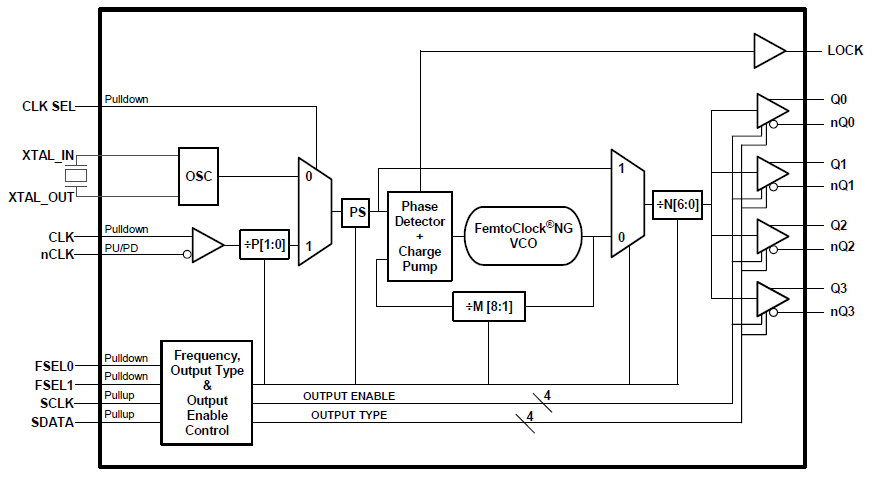
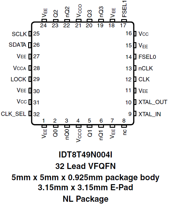
8T49N004I - Block Diagram
説明
The 8T49N004I is a four output Clock Generator with selectable LVDS or LVPECL outputs. The 8T49N004I can generate any one of four frequencies from a single crystal or reference clock. The four frequencies are selected from the Frequency Selection Table (Table 3A) and are programmed via I2C interface. The four predefined frequencies are selected in the user application by two frequency selection pins. Note the desired programmed frequencies must be used with the corresponding crystal as indicated in Table 3A. Excellent phase noise performance is maintained with Renesas' 4TH Generation FemtoClock™ NG PLL technology.
パラメータ
| 属性 | 値 |
|---|---|
| Outputs (#) | 4 |
| Output Type | LVPECL, LVDS |
| Output Freq Range (MHz) | 15.16 - 1250 |
| Input Freq (MHz) | 10 - 312.5 |
| Inputs (#) | 2 |
| Input Type | Crystal, LVPECL, LVDS, HCSL |
| Output Banks (#) | 1 |
| Core Voltage (V) | 3.3V, 2.5V |
| Output Voltage (V) | 3.3V, 2.5V |
| Feedback Input | No |
| Product Category | FemtoClock NG, Ultra-Low Jitter Clocks (<300 fs RMS), Programmable Clocks |
| Selection Criteria | 2.5V |
パッケージオプション
| Pkg. Type | Pkg. Dimensions (mm) | Lead Count (#) | Pitch (mm) |
|---|---|---|---|
| VFQFPN | 5.0 x 5.0 x 0.9 | 32 | 0.5 |


