
特長
- 5V operation
- 2xQ output, Q/2 output, Q output
- Outputs tri-state while RST low
- Internal loop filter RC network
- Low noise TTL level outputs
- < 500ps output skew, Q0-Q4
- PLL disable feature for low frequency testing
- Balanced Drive Outputs ± 24mA
- 132MHz maximum frequency (2xQ output)
- Functional equivalent to Motorola MC88915
- ESD > 2000V
- Latch-up > –300mA
- Available in QSOP and PLCC packages
- Not Recommended for New Design
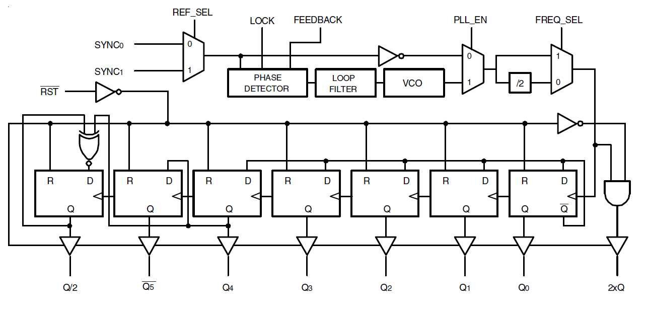
説明
The QS5917T Clock Driver uses an internal phase locked loop (PLL) to lock low skew outputs to one of two reference clock inputs. Eight outputs are available: Q0-Q4, 2xQ, Q/2, Q5. Careful layout and design insures < 500ps skew between the Q0-Q4, and Q/2 outputs. The QS5917T includes an internal RC filter which provides excellent jitter characteristics and eliminates the need for external components. In addition, TTL level outputs reduce clock signal noise. Various combinations of feedback and a divide-by-2 in the VCO path allow applications to be customized for linear VCO operation over a wide range of input SYNC frequencies. The VCO can also be disabled by the PLL_EN signal to allow low frequency or DC testing. The LOCK output asserts to indicate when phase lock has been achieved. The QS5917T is designed for use in high-performance workstations, multi-board computers, networking hardware, and mainframe systems. Several can be used in parallel or scattered throughout a system for guaranteed low skew, system-wide clock distribution networks. For more information on PLL clock driver products, see Application Note AN-227.