
特長
- Fully integrated PLL
- Eleven LVCMOS / LVTTL outputs, 7? typical output impedance
- LVCMOS / LVTTL REF_CLK input
- Output frequency range up to 180MHz at VDD = 3.3V ± 5%
- VCO range: 240MHz - 480MHz
- External feedback for "zero delay" clock regeneration
- Cycle-to-cycle jitter: 100ps (maximum)
- 3.3V supply voltage
- -40°C to 85°C ambient operating temperature
- Available in lead-free (RoHS 6) packages
説明
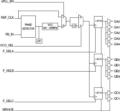
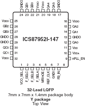
The 87952I-147 is a low voltage, low skew LVCMOS/LVTTL Clock Generator and a member of the family of High Performance Clock Solutions from IDT. With output frequencies up to 180MHz, the 87952I-147 is targeted for high performance clock applications. Along with a fully integrated PLL, the 87952I-147 contains frequency configurable outputs and an external feedback input for regenerating clocks with "zero delay". For test and system debug purposes, the nPLL_EN input allows the PLL to be bypassed. When HIGH, the MR/nOE input resets the internal dividers and forces the outputs to the high impedance state. The low impedance LVCMOS/LVTTL outputs of the 87952I- 147 are designed to drive terminated transmission lines. The effective fanout of each output can be doubled by utilizing the ability of each output to drive two series terminated transmission lines.