特長
- Enhanced N-channel FET with no inherent diode to Vcc
- Pin compatible with the 74'125 function
- Undershoot clamp diodes on all switch and control inputs
- Hot-swapping, hot-docking
- Voltage translation (5V to 3.3V)
- Power conservation
- Capacitance reduction and isolation (mass storage, workstations)
- Logic replacement (data processing)
- Clock gating
- Bus isolation
- Available in 16-pin QSOP and 14-pin SOIC packages
説明
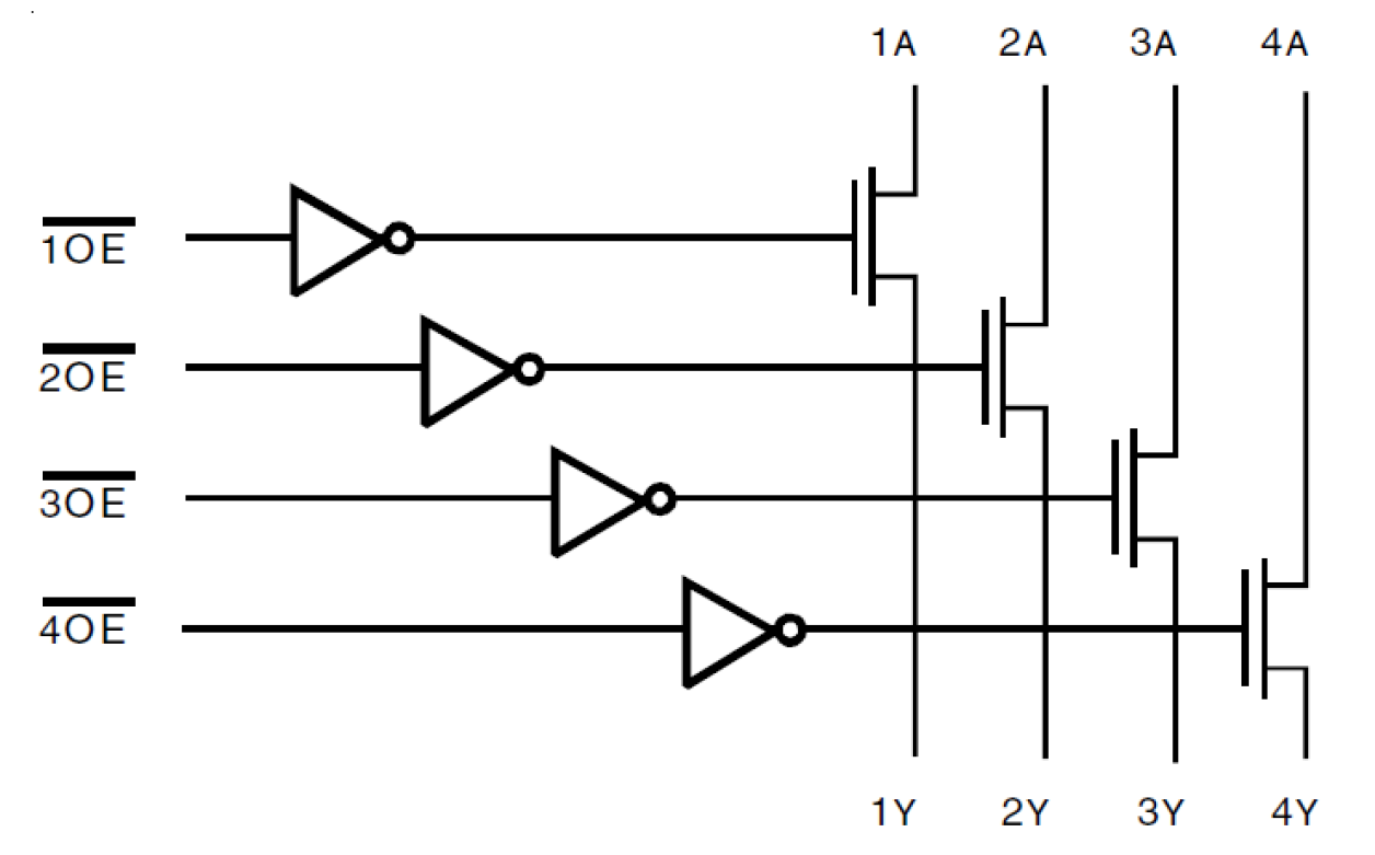
The QS3125 provides a set of four high-speed low-resistance CMOS switches connecting inputs to outputs without propagation delay and without generating additional ground bounce noise. The QS3125 is ideal for signal and control switching since the device adds no noise, ground bounce, propagation delay, or significant power consumption to the system. The QS3125 can also be used for analog switching applications such as video. The device operates at -40 °C to +85 °C.
パラメータ
| 属性 | 値 |
|---|---|
| Function | Bus Switch |
| Pkg. Code | PCG16 |
| Temp. Range (°C) | -40 to 85°C |
| Bus Width (bits) | 4 |
| Core Voltage (V) | 5 |
| On Resistance (Ω) | 5 |
| Speed Grade | Standard |
パッケージオプション
| Pkg. Type | Pkg. Dimensions (mm) | Lead Count (#) | Pitch (mm) |
|---|---|---|---|
| QSOP | 4.9 x 3.8 x 1.47 | 16 | 0.64 |
適用されたフィルター

