
パッケージ情報
| CADモデル: | View CAD Model |
| Pkg. Type: | TSSOP |
| Pkg. Code: | PGG8 |
| Lead Count (#): | 8 |
| Pkg. Dimensions (mm): | 3.1 x 4.4 x 1.0 |
| Pitch (mm): | 0.65 |
環境及び輸出分類情報
| Moisture Sensitivity Level (MSL) | 1 |
| Pb (Lead) Free | Yes |
| ECCN (US) | EAR99 |
| HTS (US) | 8542.39.0090 |
製品スペック
| Lead Count (#) | 8 |
| Carrier Type | Reel |
| Moisture Sensitivity Level (MSL) | 1 |
| Qty. per Reel (#) | 2500 |
| Qty. per Carrier (#) | 0 |
| Package Area (mm²) | 13.6 |
| Pitch (mm) | 0.65 |
| Pkg. Dimensions (mm) | 3.1 x 4.4 x 1.0 |
| Pb (Lead) Free | Yes |
| Pb Free Category | e3 Sn |
| Temp. Range (°C) | 0 to 70°C |
| C-C Jitter Max P-P (ps) | 200 |
| Core Voltage (V) | 3.3 |
| Input Freq (MHz) | 10 - 133 |
| Input Type | LVCMOS |
| Inputs (#) | 1 |
| Length (mm) | 3.1 |
| MOQ | 2500 |
| Output Banks (#) | 2 |
| Output Freq Range (MHz) | 10 - 133 |
| Output Signaling | LVCMOS |
| Output Skew (ps) | 250 |
| Output Type | LVCMOS |
| Output Voltage (V) | 3.3 |
| Outputs (#) | 5 |
| Pkg. Type | TSSOP |
| Product Category | Zero Delay Buffers |
| Reel Size (in) | 13 |
| Requires Terms and Conditions | Does not require acceptance of Terms and Conditions |
| Tape & Reel | Yes |
| Thickness (mm) | 1 |
| Width (mm) | 4.4 |
MPC962305 に関するリソース
説明
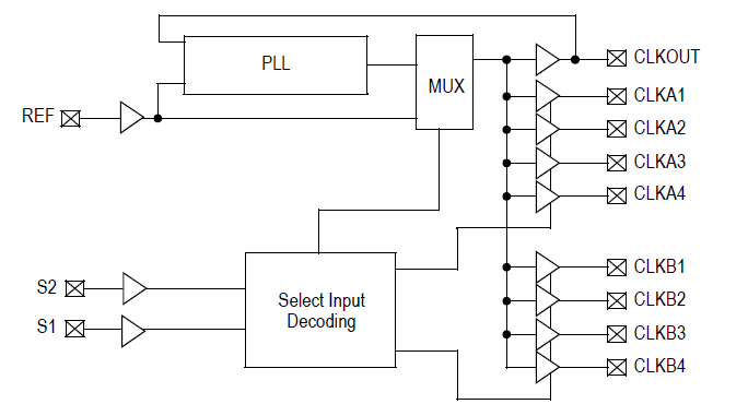
The MPC962309 has two banks of four outputs each, which can be controlled by the Select Inputs as shown in Table 3. Bank B can be tri-stated if all of the outputs are not required. Select inputs also allow the input clock to be directly applied to the outputs for chip and system testing purposes. The MPC962305 and MPC962309 PLLs enters a power down state when there are no rising edges on the REF input. During this state, all of the outputs are in tristate, the PLL is turned off, and there is less than 25.0 ?A of current draw for the device. The PLL shuts down in one additional case as shown in Table 3. Multiple MPC962305 and MPC962309 devices can accept the same input clock and distribute it throughout the system. In this situation, the difference between the output skews of two devices will be less than 700 ps. All outputs have less than 200 ps of cycle-cycle jitter. The input-to-output propagation delay on both devices is guaranteed to be less than 350 ps and the output-to-output skew is guaranteed to be less than 250 ps. The MPC962305 and MPC962309 are available in two/three different configurations, as shown on the ordering information page. The MPC962305-1/MPC962309-1 are the base parts. High drive versions of those devices, MPC962305-1H and MPC962309-1H, are available to provide faster rise and fall times of the base device.