
| CADモデル: | View CAD Model |
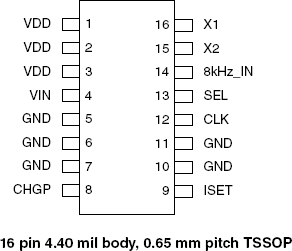
| Pkg. Type: | TSSOP |
| Pkg. Code: | PGG16 |
| Lead Count (#): | 16 |
| Pkg. Dimensions (mm): | 5.0 x 4.4 x 1.0 |
| Pitch (mm): | 0.65 |
| Pb (Lead) Free | Yes |
| ECCN (US) | EAR99 |
| HTS (US) | 8542.39.0090 |
| Moisture Sensitivity Level (MSL) | 1 |
| Pkg. Type | TSSOP |
| Lead Count (#) | 16 |
| Pb (Lead) Free | Yes |
| Carrier Type | Tube |
| Abs. Pull Range Min. (± PPM) | 115 |
| C-C Jitter Typ P-P (ps) | 150 |
| Core Voltage (V) | 3.3 |
| Feedback Input | No |
| Input Freq (MHz) | 0.008 - 0.008 |
| Input Type | LVCMOS |
| Inputs (#) | 1 |
| Length (mm) | 5 |
| MOQ | 96 |
| Moisture Sensitivity Level (MSL) | 1 |
| Output Banks (#) | 1 |
| Output Freq Range (MHz) | 1.544 - 1.544, 2.048 - 2.048 |
| Output Type | LVCMOS |
| Output Voltage (V) | 3.3 |
| Outputs (#) | 1 |
| Package Area (mm²) | 22 |
| Pb Free Category | e3 Sn |
| Pitch (mm) | 0.65 |
| Pkg. Dimensions (mm) | 5.0 x 4.4 x 1.0 |
| Prog. Clock | No |
| Qty. per Carrier (#) | 96 |
| Qty. per Reel (#) | 0 |
| Requires Terms and Conditions | Does not require acceptance of Terms and Conditions |
| Tape & Reel | No |
| Temp. Range (°C) | -40 to 85°C |
| Thickness (mm) | 1 |
| Width (mm) | 4.4 |
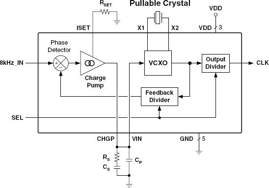
The MK1581-01 provides synchronization and timing control for T1 and E1 based network access or multitrunk telecommunication systems. The device accepts an 8 kHz frame clock input and uses an on-chip VCXO to produce a synchronized low phase noise clock output. This monolithic IC, combined with an external inexpensive quartz crystal, can be used to replace a more costly hybrid VCXO retiming module. Through selection of external loop filter components values, the device can be tailored to meet the system's clock jitter attenuation requirements. Low-pass jitter attenuation characteristics in the Hz range are possible.