パッケージ情報
| CADモデル: | View CAD Model |
| Pkg. Type: | DIE |
| Pkg. Code: | |
| Lead Count (#): | |
| Pkg. Dimensions (mm): | |
| Pitch (mm): |
環境及び輸出分類情報
| Moisture Sensitivity Level (MSL) | |
| Pb (Lead) Free | No |
| ECCN (US) | EAR99 |
| HTS (US) | 8542.39.0090 |
| RoHS (IS0-1825BSRH-Q) | 英語日本語 |
製品スペック
| Pkg. Type | DIE |
| DLA SMD | 5962F0251103V9A |
| Pb (Lead) Free | No |
| MOQ | 100 |
| Temp. Range (°C) | -55 to +125°C |
| CAGE code | 34371 |
| Control Mode | Voltage, Peak Current Mode |
| DSEE (MeV·cm2/mg) | 86.3 |
| Die Sale Availability? | No |
| Duty Cycle (Max) (%) | 50 |
| Flow | RH Hermetic |
| Lead Compliant | No |
| Models Available | iSIM |
| No-Load Operating Current | 25 mA |
| Operating Freq (Max) (MHz) | 0.5 |
| PROTO Availability? | No |
| Phase of Outputs | Out of Phase |
| Phases (Max) | 2 |
| Qualification Level | Class V |
| Quiescent Current | 55µA |
| Rating | Space |
| SMD URL | 5962-02511 |
| Supply Voltage (max) (V) | 30 - 30 |
| Supply Voltage (min) (V) | 12 - 12 |
| Switching Frequency (max) (kHz) | 3000 |
| Switching Frequency (min) (kHz) | 10 |
| TID HDR (krad(Si)) | 300 |
| Tape & Reel | No |
| Topology | Boost, Flyback, Forward, Full Bridge, Half Bridge, Push-Pull |
| UVLO Rising (V) | 8.6 |
| VDD1 (V) | 12 - 20 |
| VREF (V) | 5.1 |
IS-1825BSRH に関するリソース
説明
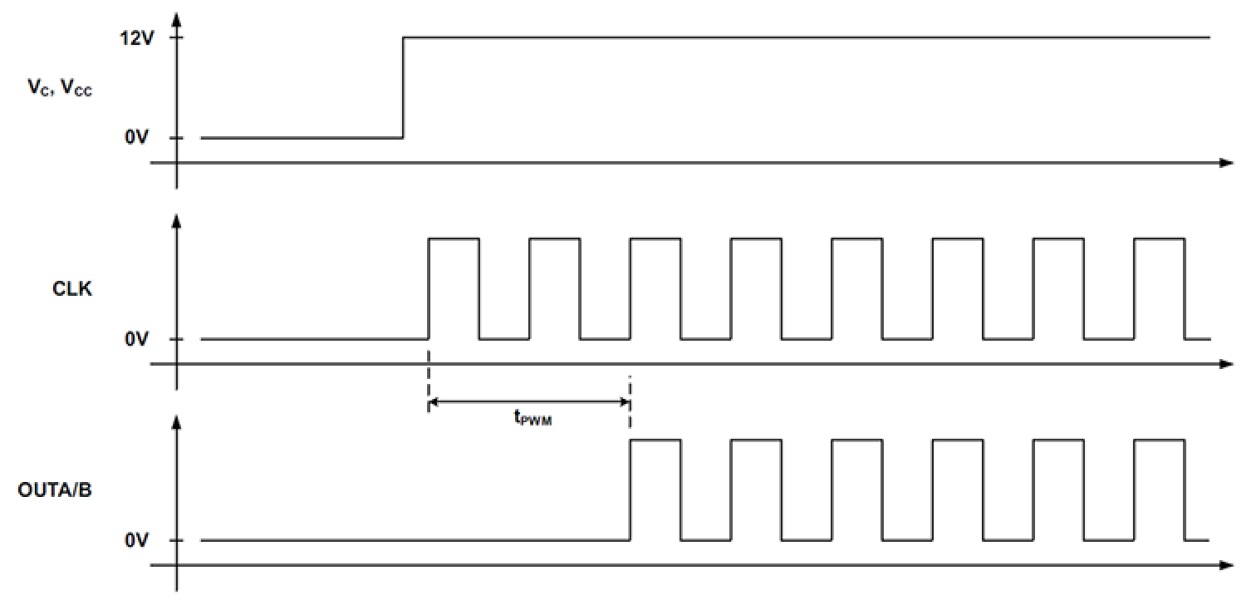
The IS-1825ASRH, IS-1825BSRH, IS-1825BSEH, ISL71823ASRH, and ISL71823BSRH are single event and total dose hardened pulse width modulators designed to be used in high-frequency switching power supplies in either voltage or current-mode configurations. These devices include a precision voltage reference, a low power start-up circuit, a high-frequency oscillator, a wide-band error amplifier, and a fast current-limit comparator. The IS-1825xSRH and IS-1825xSEH feature dual, alternating output operating from zero to less than 50% duty cycle, and the ISL71823xSRH features dual in-phase output operating from zero to less than 100% duty cycle. The B versions of the parts test the delay from clock out to PWM output switching after power has been applied to the modulator (tPWM). The SEH parts are wafer-by-wafer acceptance tested to 50krad(Si) at a low dose rate of <10mrad(Si)/s. Constructed with the Rad Hard Silicon Gate (RSG) dielectrically isolated BiCMOS process, these devices are immune to single-event latch-up and have been specifically designed to provide a high level of immunity to single-event transients. All specified parameters are established and tested for 300krad(Si) total dose performance. The devices are offered in a 16 Ld CDIP or a 20 Ld CDFP and fully specified to across the temperature range of -50 °C to +125 °C.
