特長
- 終端の内蔵により100Ωの差動Zoを実現、部品点数と基板面積の削減を実現
- 1.8V動作、低消費電力化
- OE#ピン、DIFパワーマネージメント対応
- LP-HCSL差動クロック出力、消費電力と基板面積を削減
- 各出力のプログラマブルスルー・レート:様々な線長に合わせたチューニングが可能
- プログラマブル出力振幅:様々な使用環境に合わせたチューニングが可能
- PLLがロックされるまでのDIF出力ブロック:クリーンシステムスタートアップ
- 0%、-0.25%、-0.5%から選択可能なDIF出力スプレッド:EMIの低減
- 外付け25MHz水晶振動子、0ppmの合成エラーでタイトなppmをサポート
- ストラップピンによるコンフィギュレーションが可能:デバイス制御のためのSMBusインターフェースは不要
- レガシーコントローラ対応3.3V SMBus インターフェース
- 省スペース5×5mm 32ピンVFQFPN、最小限の基板スペースを実現
- 選択可能なSMBusアドレス:複数のデバイスでSMBusセグメントを簡単に共有可能

9FGV0441 - Block Diagram
説明
9FGV0441は、PCIe Gen1-4アプリケーション用の4出力超低消費電力クロックジェネレータで、Zo = 100Ωの出力終端を内蔵しています。 クロック管理用に4つの出力イネーブルを備え、スペクトラム拡散オフに加えて、2種類のスペクトラム拡散レベルをサポートします。
パラメータ
| 属性 | 値 |
|---|---|
| Diff. Outputs | 4 |
| Diff. Output Signaling | LP-HCSL |
| Output Freq Range (MHz) | 25 - 25, 100 - 100 |
| Power Consumption Typ (mW) | 58 |
| Supply Voltage (V) | 1.8 - 1.8 |
| Output Type | LP-HCSL, LVCMOS |
| Xtal Freq (MHz) | 25 - 25 |
| Diff. Termination Resistors | 0 |
| Package Area (mm²) | 25 |
| Battery Backup | No |
| Battery Seal | No |
| CPU Supervisory Function POR | No |
| Crystal Frequency Trimming | No |
| Frequency Out Pin | No |
| Inputs (#) | 1 |
| Input Freq (MHz) | 25 - 25 |
| Function | Generator |
| Input Type | Crystal, LVCMOS |
| Core Voltage (V) | 1.8 |
| Output Voltage (V) | 0.8V, 1.8V |
| Product Category | PCI Express Clocks |
パッケージオプション
| Pkg. Type | Pkg. Dimensions (mm) | Lead Count (#) | Pitch (mm) |
|---|---|---|---|
| VFQFPN | 5.0 x 5.0 x 0.9 | 32 | 0.5 |
アプリケーション・ブロック図
 | RZ/G2E搭載SoM用パワー&タイミングソリューション 最適な電源とタイミングツリーを搭載した SoM は、正確なタイミングと効率的な電力分配を保証します。 |
このデバイスに組み合わせたい製品
更に設計開発を進めるための製品を探してみましょう
Renesas Boards & Kits

RZ/N2H-EVKIT
アクティブ
RZ/N2H Evaluation Board Kit
RZ/N2H Evaluation Board Kitは、RZ/N2H MPUの評価・開発キットです。オンボードエミュレータを搭載しているので、付属のケーブルをPCに接続するだけで評価を開始できます。ギガビットイーサネットPHY、不揮発性メモリ、LPDDR4メモリなど豊富な機能を持つICを搭載しており、拡張ボードなしでRZ/N2Hの様々な機能を評価することができます。
また、インバータボードを拡張することで、多軸モータ制御を実現することも可能です。
Partner Boards & Kits
SoM/SBC
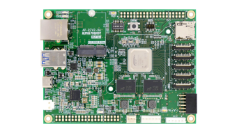
AP-RZV2-0A
Provides a CPU board equipped with the Renesas RZ/V2H. The RZ/V2H integrates a quad-core Arm® Cortex®-A55 with dual Arm® Cortex®-R8 cores, along with an AI accelerator and programmable hardware DRP, enabling fanless AI inference performance of up to 80 TOPS. Supports interfaces including Gigabit Ethernet, USB3.2 Gen2, M.2, microSD, MIPI CSI-2, and MIPI DSI, making it suitable for autonomous systems and FA machine vision applications requiring advanced AI processing.
Provided By:
株式会社アルファプロジェクト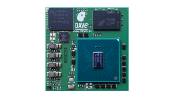
SoM/SBC
RZ/T2H ZERO SOM
The ZERO SOM, developed by DAVE Embedded Systems, is a system on module (SoM) featuring the Renesas RZ/T2H application processor. This SOM is part of the Harsh Line portfolio from DAVE Embedded Systems, which ensures maximum performance and integration. With a minimum availability of 15 years, it meets the needs of reliable and durable industrial applications. ZERO SOM includes up to 3 industrial MAC Ethernet ports, up to 9 motor control axes, and a safety management system, making it ideal for industrial, safe, and secure connected applications.
Provided By:
DAVE Embedded Systems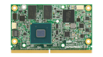
SoM/SBC
SMARC RZ/G2E System on Module (SoM)
Provides a System on Module (SoM) based on the Renesas RZ/G2E. Delivers dual Arm® Cortex®-A53 processing with an integrated PowerVR GE8300 3D graphics engine and supports Full HD video encoding and decoding. Supports high-speed interfaces such as PCI Express and display connectivity, making it suitable for HMI applications. Complies with the SMARC 2.1 standard form factor to enable flexible and scalable system design with high compatibility and expandability.
Provided By:
株式会社アルファプロジェクト