特長
- Device clock domain (RF-PLL) with support for JESD204B/C
- Digital clock domain (Ethernet, FEC) with support for eEEC and T-BC/T-TSC Class C
- 2 differential clock reference inputs with 1PPS (1Hz) to 1GHz input frequency
- Dual DPLL front-end with independent clock paths
- External control of the DCO for IEEE1588
- Digital holdover with a 1.1 × 10⁻⁷ ppb accuracy
- Programmable DPLL loop bandwidth 1mHz - 6kHz
- Configurable phase delay (range: 1UI)
- Hitless input switching with < 1ns output phase error
- Reference monitors for input LOS, activity and frequency
- 1 external synchronization input for JESD204B/C (LVCMOS)
- 16 differential outputs
- Optimized for low phase noise: -146dBc/Hz (1MHz offset; 245.76MHz clock)
- Supply voltage (core): 3.3V; (outputs): 3.3V, 2.5V, and 1.8V
- Board temperature range: -40°C to +105°C
- Applicable Standards
- ITU-T G.8262 EEC1/2, G.8262.1 eEEC
- ITU-T G.8273.2 T-BC/T-TSC Class C
- JESD204B and C


説明
8V19N850は、無線基地局無線装置の位相/周波数同期と信号調整用の高性能クロックソリューションとして設計された完全一体型の無線ユニットクロックシンクロナイザおよびジッタ減衰器です。 このデバイスは、JESD204B/C サブクラス0および1のデバイスクロックとコンバータ用のSYSREF同期をサポートしています。 8V19N850は、4出力でデジタルクロック(EthernetおよびFECレート)ドメインに使用できるものと、12出力でデバイスクロック(RF-PLL)ドメインに使用できるものの、2つの独立した周波数ドメインをサポートしています。 イーサネットドメインは、2つのAPLLから周波数を生成し、柔軟に対応します。RFクロックドメイン出力は、ADC/DAC回路用の超低位相ノイズクロックを生成します。
内蔵RF-PLLから、ADC/DACデバイスの低周波同期信号(SYSREF)を駆動するための高周波デバイスクロックの生成に対応しています。 デュアルDPLLフロントエンドアーキテクチャは、周波数変換をサポートします。 各DPLLはプログラマブルな帯域幅と、リアルタイムに周波数/位相を調整するDCO機能を備えています。 DPLLは1PPSの入力信号に対してロックすることができ、100秒以内にロックを確立することができます。 DPLL-0からDPLL-1へ、またはその逆方向の周波数情報を適用することで、2つのリファレンス周波数特性を合成することができます(コンボモード)。 8V19N850は、ピンマップされたI3C(レガシーI2Cを含む)および3/4線式SPIインタフェースによって設定されます。 マスタ機能を持つI2Cは、外部ROMデバイスからデフォルトコンフィギュレーションを読み出します。 GPIOポートは、レポートや制御用に設定することができます。
パラメータ
| 属性 | 値 |
|---|---|
| Output Freq Range (MHz) | 1.0E-6 - 1000 |
| Accepts Spread Spec Input | No |
| Supply Voltage (V) | 3.3 - 3.3, 2.5 - 2.5, 1.8 - 1.8 |
| Output Type | LVDS, LVPECL, LVCMOS |
| Battery Backup | No |
| Battery Seal | No |
| CPU Supervisory Function POR | No |
| Crystal Frequency Trimming | No |
| Frequency Out Pin | No |
| Inputs (#) | 2 |
| Input Freq (MHz) | 1.0E-6 - 1000 |
| DPLL Channels (#) | 2 |
| JESD204B/C Compliant | Yes |
| Frequency Plan | 2500 / Output_Divider, 2949.12 / Output_Divider, 3670-3868 / Output_Divider |
| Adjustable Phase | Yes |
| Noise Floor (dBc/Hz) | -165 |
| Phase Noise Supports GSM | Yes |
| Synthesis Mode | Integer, Fractional |
| Input Ref. Divider Resolution (bits) | 3 |
| Feedback Divider Resolution (bits) | 32 |
| Output Divider Resolution (bits) | 7 |
| Input Redundancy | Input Monitor, Digital holdover, Hitless switch, Phase-slope limiting |
| Channels (#) | 1 |
| Additive Phase Jitter Typ RMS (fs) | 52 |
| Grade | 5G |
| Output Banks (#) | 8 |
| Core Voltage (V) | 1.8 |
| Output Voltage (V) | 1.8V, 2.5V, 3.3V |
| Product Category | JESD204B/C |
パッケージオプション
| Pkg. Type | Pkg. Dimensions (mm) | Lead Count (#) | Pitch (mm) |
|---|---|---|---|
| VFQFPN | 10.0 x 10.0 x 0.9 | 88 | 0.4 |
アプリケーション
- Wireless infrastructure 5G radio
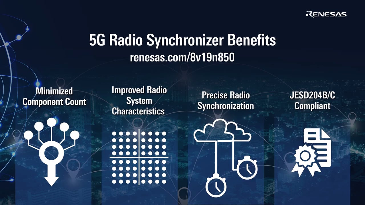
This video introduces the industry’s first fully-integrated synchronizer for 5G enhanced common public radio interface (eCPRI) radio synchronization.