
| CADモデル: | View CAD Model |
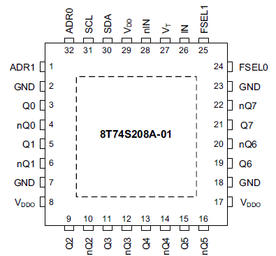
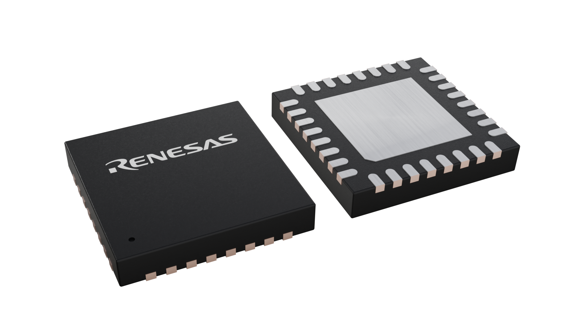
| Pkg. Type: | VFQFPN |
| Pkg. Code: | NLG32 |
| Lead Count (#): | 32 |
| Pkg. Dimensions (mm): | 5.0 x 5.0 x 0.9 |
| Pitch (mm): | 0.5 |
| Moisture Sensitivity Level (MSL) | 3 |
| Pb (Lead) Free | Yes |
| ECCN (US) | EAR99 |
| HTS (US) | 8542.39.0090 |
| Lead Count (#) | 32 |
| Carrier Type | Tray |
| Moisture Sensitivity Level (MSL) | 3 |
| Qty. per Reel (#) | 0 |
| Qty. per Carrier (#) | 490 |
| Pb (Lead) Free | Yes |
| Pb Free Category | e3 Sn |
| Temp. Range (°C) | -40 to 85°C |
| Additive Phase Jitter Typ RMS (fs) | 96 |
| Additive Phase Jitter Typ RMS (ps) | 0.096 |
| Adjustable Phase | No |
| Advanced Features | Individual output enable, I2C, Per-bank divider |
| Channels (#) | 1 |
| Core Voltage (V) | 2.5 |
| Divider Value | 1, 2, 4, 8 |
| Function | Buffer, Divider |
| Input Freq (MHz) | 1000 |
| Input Type | CML, LVDS, LVPECL |
| Inputs (#) | 1 |
| Length (mm) | 5 |
| MOQ | 490 |
| Noise Floor (dBc/Hz) | -152 |
| Output Banks (#) | 1 |
| Output Freq Range (MHz) | 1000, 500, 250, 125 |
| Output Skew (ps) | 45 |
| Output Type | LVDS |
| Output Voltage (V) | 2.5 |
| Outputs (#) | 8 |
| Package Area (mm²) | 25 |
| Pitch (mm) | 0.5 |
| Pkg. Dimensions (mm) | 5.0 x 5.0 x 0.9 |
| Pkg. Type | VFQFPN |
| Product Category | Clock Buffers & Drivers, RF Buffers |
| Requires Terms and Conditions | Does not require acceptance of Terms and Conditions |
| Supply Voltage (V) | 2.5 - 2.5, 3.3 - 3.3 |
| Tape & Reel | No |
| Thickness (mm) | 0.9 |
| Width (mm) | 5 |
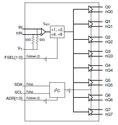
The 8T74S208A-01 is a high-performance differential LVDS clock divider and fanout buffer. The device is designed for the frequency division and signal fanout of high-frequency, low phase noise clocks. The 8T74S208A-01 is characterized to operate from a 2.5V power supply. Guaranteed output-to-output and part-to-part skew characteristics make the 8T74S208A-01 ideal for those clock distribution applications demanding well-defined performance and repeatability. The integrated input termination resistors make interfacing to the reference source easy and reduce passive component count. Each output can be individually enabled or disabled in the high-impedance state controlled by an I²C register. On power-up, all outputs are disabled.