
特長
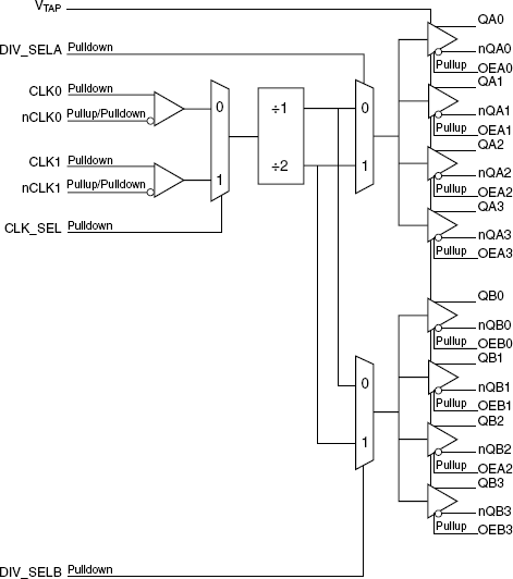
- Eight differential LVDS output pairs Each output has individual synchronous output enable
- Two selectable differential CLKx, nCLKx input pairs
- CLKx, nCLKx pairs can accept the following differential input levels: LVPECL, LVDS, HCSL
- Maximum output frequency: 1.5GHz
- Independent bank control for ÷1 or ÷2 operation
- Glitchless output behavior during input switch
- Output skew: 40ps (maximum)
- Bank skew: 35ps (maximum)
- Full 3.3V or 2.5V supply mode
- -40°C to 85°C ambient operating temperature
- Available in lead-free (RoHS 6) package
説明
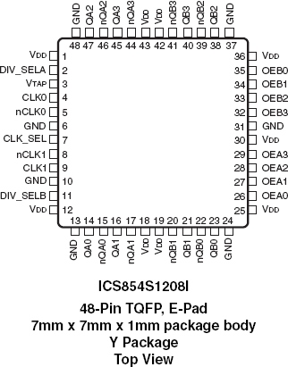
The 854S1208I is a low skew, 8 output LVDS Fanout Buffer with selectable divider. The 854S1208I has 2 selectable inputs that accept a variety of differential input types. The device provides the capability to suppress any glitch at the outputs of the device during an input clock switch to enhance clock redundancy in fault tolerant applications. The divide select inputs, DIV_SELA and DIV_SELB, control the output frequency of each bank. The output banks can be independently selected for ÷1 or ÷2 operation. The output enable pins assigned to each output, support enabling and disabling each output individually. The 854S1208I is characterized at full 3.3V or 2.5V output operating supply modes. Guaranteed output and part-to-part skew characteristics make the 854S1208I ideal for high performance applications.