
特長
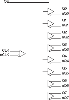
- Eight differential LVDS output pairs
- One differential clock input pair
- CLK/nCLK can accept the following differential input levels: LVPECL, LVDS, LVHSTL, HCSL, SSTL
- Maximum output frequency: 700MHz
- Translates any differential input signal (LVPECL, LVHSTL, SSTL, HCSL) to LVDS levels without external bias networks
- Translates any single-ended input signal to LVDS with resistor bias on nCLK input
- Multiple output enable inputs for disabling unused outputs in reduced fanout applications
- Additive phase jitter, RMS: 167fs (typical)
- Output skew: 50ps (maximum)
- Part-to-part skew: 550ps (maximum)
- Propagation delay: 2.4ns (maximum)
- 3.3V operating supply
- -40°C to 85°C ambient operating temperature
- Available in lead-free (RoHS 6) package
説明
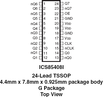
The 85408I is a low skew, high performance 1-to-8 Differential-to-LVDS Clock Distribution Chip and a member of the family of High Performance Clock Solutions from IDT. The 85408I CLK, nCLK pair can accept most differential input levels and translates them to 3.3V LVDS output levels. Utilizing Low Voltage Differential Signaling (LVDS), the 85408I provides a low power, low noise, low skew, point-to-point solution for distributing LVDS clock signals. Guaranteed output and part-to-part skew specifications make the 85408I ideal for those applications demanding well defined performance and repeatability.