
特長
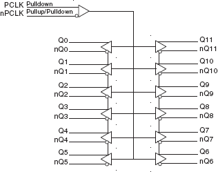
- Twelve differential 3.3V, 2.5V LVPECL outputs
- PCLK, nPCLK input pair
- PCLK, nPCLK pair can accept the following differential input levels: LVPECL, CML, SSTL
- Maximum output frequency: 1.5GHz
- Translates any single-ended input signal to 2.5V or 3.3V LVPECL levels with a resistor bias on nPCLK input
- Additive phase jitter, RMS: 0.06ps (typical)
- Output skew: 50ps (maximum)
- Part-to-part skew: 250ps (maximum)
- Propagation delay: 680ps (maximum)
- Full 3.3V or 2.5V operating supply modes
- -40°C to 85°C ambient operating temperature
- Available in lead-free (RoHS 6) package
説明
The 853S12I is a low skew, 1-to-12 Differential-to- 3.3V, 2.5V LVPECL Fanout Buffer and a member of the HiPerClockS™ family of High Performance Clock Solutions from IDT. The PCLK, nPCLK pair accepts LVPECL, CML, and SSTL differential input levels. The high gain differential amplifier accepts peak-to-peak input voltages as small as 150mV, as long as the common mode voltage is within the specified minimum and maximum range. Guaranteed output and part-to-part skew characteristics make the 853S12I ideal for those clock distribution applications demanding well defined performance and repeatability.
パラメータ
| 属性 | 値 |
|---|---|
| Temp. Range (°C) | -40 to 85°C |
| Product Category | Clock Buffers & Drivers, RF Buffers |
パッケージオプション
| Pkg. Type | Pkg. Dimensions (mm) | Lead Count (#) | Pitch (mm) |
|---|---|---|---|
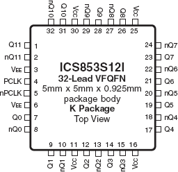
| VFQFPN | 5.0 x 5.0 x 0.9 | 32 | 0.5 |