
特長
- One 0.7V current mode differential HCSL output pair
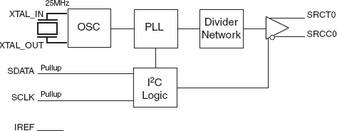
- Crystal oscillator interface: 25MHz
- Output frequency: 100MHz
- RMS period jitter: 3ps (maximum)
- Cycle-to-cycle jitter: 35ps (maximum)
- I2C support with readback capabilities up to 400kHz
- Spread Spectrum for electromagnetic interference (EMI) reduction
- 3.3V operating supply mode
- 0°C to 70°C ambient operating temperature
- Available in lead-free (RoHS 6) package
説明
The 841S01 is a PLL-based clock generator specifically designed for PCI_Express™ Clock Generation applications. This device generates a 100MHz HCSL clock. The device offers a HCSL (Host Clock Signal Level) clock output from a clock input reference of 25MHz. The input reference may be derived from an external source or by the addition of a 25MHz crystal to the on-chip crystal oscillator. An external reference may be applied to the XTAL_IN pin with the XTAL_OUT pin left floating. The device offers spread spectrum clock output for reduced EMI applications. An I2C bus interface is used to enable or disable spread spectrum operation as well as select either a down spread value of -0.35% or -0.5%.
パラメータ
| 属性 | 値 |
|---|---|
| Diff. Outputs | 1 |
| App Jitter Compliance | PCIe Gen1, PCIe Gen2, PCIe Gen3 |
| Outputs (#) | 1 |
| Output Type | HCSL |
| Output Freq Range (MHz) | 100 - 100 |
| Input Freq (MHz) | 25 - 25 |
| Inputs (#) | 1 |
| Input Type | Crystal |
| Output Banks (#) | 1 |
| Core Voltage (V) | 3.3 |
| Output Voltage (V) | 3.3 |
| Product Category | PCI Express Clocks |
パッケージオプション
| Pkg. Type | Pkg. Dimensions (mm) | Lead Count (#) | Pitch (mm) |
|---|---|---|---|
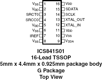
| TSSOP | 5.0 x 4.4 x 1.0 | 16 | 0.65 |