
特長
- Five single-ended LVCMOS/LVTTL outputs
- Two REF_OUT LVCMOS/LVTTL clock outputs
- Selectable crystal oscillator interface, 25MHz, 18pF parallel resonant crystal or LVCMOS/LVTTL single-ended reference input
- Supports the following output frequencies: Output QAA/Bank B: 33.33MHz, 50MHz, 66.67MHz, 83.33MHz, 100MHz, 125MHz, 133.33MHz and 166.67MHz Output QAB: 125MHz
- VCO frequency: 2GHz
- Slew rate control
- Voltage supply modes: Core/Output 3.3V/3.3V 3.3V/2.5V
- -40°C to 85°C ambient operating temperature
- Available in lead-free (RoHS 6) package
説明
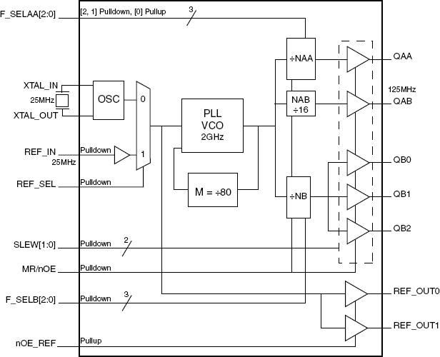
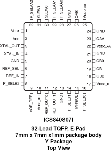
The 840S07I is a seven output LVCMOS/LVTTL Frequency Synthesizer accepting crystal or single-ended reference clock inputs. The 840S07I uses a 25MHz parallel resonant crystal to generate 33.33MHz – 166.67MHz clock signals, replacing solutions requiring multiple oscillator and fanout buffer solutions. The device supports output slew rate control with two slew select pins (SLEW[1:0]). The VCO operates at a frequency of 2GHz. The device has 3 output banks, output QAA with one 33.33MHz – 166.67MHz LVCMOS/LVTTL output, output QAB with one 125MHz LVCMOS/LVTTL output and Bank B with three 33.33MHz – 166.67MHz LVCMOS/LVTTL outputs. Output QAA and Bank B have their own dedicated frequency select pins and can be independently set for the frequencies mentioned above. Designed for networking and industrial applications, the 840S07I can also drive the high-speed clock inputs of communication processors, DSPs, switches and bridges.