
特長
- Sixteen LVCMOS/LVTTL outputs, 7Ω typical output impedance
- One LVCMOS/LVTTL clock input
- CLK can accept the following input levels: LVCMOS, LVTTL
- Maximum output frequency: 200MHz
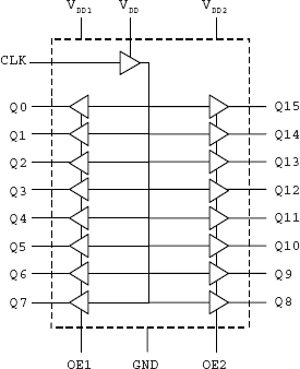
- Dual output enable inputs facilitates 1-to-16 or 1-to-8 input
- All inputs are 5V tolerant
- Output skew: 250ps (typical)
- Part-to-part skew: 700ps (typical)
- Output supply modes: Core/Output 3.3V/3.3V 2.5V/2.5V 3.3V/2.5V
- -40°C to 85°C ambient operating temperature
説明
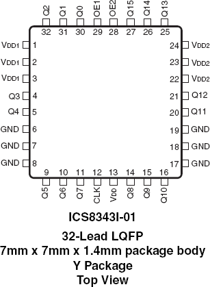
The 8343I-01 is a low skew, 1-to-16 LVCMOS/ LVTTL Fanout Buffer. The 8343I-01 single ended clock input accepts LVCMOS or LVTTL input levels. The 8343I-01 operates at 3.3V, 2.5V and mixed 3.3V input and 2.5V supply modes over the industrial temperature range. Guaranteed output and part-to-part skew characteristics make the 8343I-01 ideal for those clock distribution applications demanding well defined performance and repeatability.