パッケージ情報
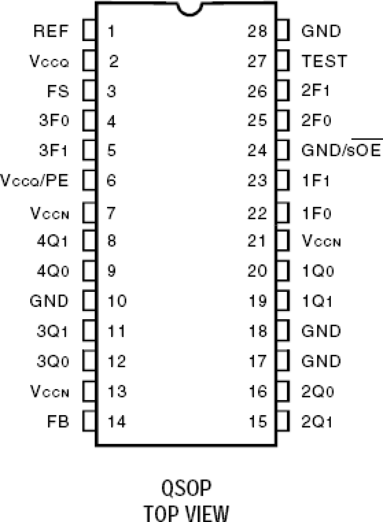
| Pkg. Type: | QSOP |
| Pkg. Code: | PCG28 |
| Lead Count (#): | 28 |
| Pkg. Dimensions (mm): | 9.9 x 3.8 x 1.47 |
| Pitch (mm): | 0.64 |
環境及び輸出分類情報
| Pb (Lead) Free | Yes |
| ECCN (US) | EAR99 |
| HTS (US) | 8542.39.0090 |
| Moisture Sensitivity Level (MSL) | 1 |
製品スペック
| Pkg. Type | QSOP |
| Lead Count (#) | 28 |
| Pb (Lead) Free | Yes |
| Carrier Type | Tube |
| Advanced Features | Programmable Clock, Feedback Input |
| C-C Jitter Max P-P (ps) | 200 |
| Core Voltage (V) | 3.3 |
| Feedback Input | Yes |
| Input Freq (MHz) | 3.75 - 85 |
| Input Type | LVCMOS |
| Inputs (#) | 1 |
| Length (mm) | 9.9 |
| MOQ | 144 |
| Moisture Sensitivity Level (MSL) | 1 |
| Output Banks (#) | 4 |
| Output Freq Range (MHz) | 3.75 - 85 |
| Output Skew (ps) | 250 |
| Output Type | LVCMOS |
| Output Voltage (V) | 3.3 |
| Outputs (#) | 8 |
| Package Area (mm²) | 37.6 |
| Pb Free Category | e3 Sn |
| Pitch (mm) | 0.64 |
| Pkg. Dimensions (mm) | 9.9 x 3.8 x 1.47 |
| Prog. Clock | No |
| Qty. per Carrier (#) | 48 |
| Qty. per Reel (#) | 0 |
| Requires Terms and Conditions | Does not require acceptance of Terms and Conditions |
| Tape & Reel | No |
| Temp. Range (°C) | -40 to 85°C |
| Thickness (mm) | 1.47 |
| Width (mm) | 3.8 |
5V993A に関するリソース
説明
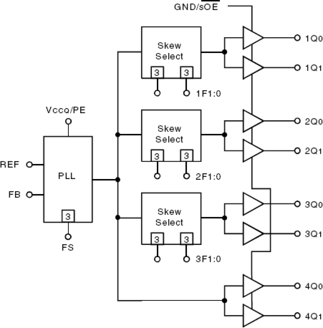
The IDT5V993A is a high fanout 3.3V PLL based clock driver intended for high performance computing and data-communications applications. A key feature of the programmable skew is the ability of outputs to lead or lag the REF input signal. The IDT5V993A has six programmable skew outputs and two zero skew outputs. Skew is controlled by 3-level input signals that may be hard-wired to appropriate HIGH-MID-LOW levels. When the GND/sOE pin is held low, all the outputs are synchronously enabled. However, if GND/sOE is held high, all the outputs except 3Q0 and 3Q1 are synchronously disabled. Furthermore, when the VCCQ/PE is held high, all the outputs are synchronized with the positive edge of the REF clock input. When VCCQ/PE is held low, all the outputs are synchronized with the negative edge of REF. Both devices have LVTTL outputs with 12mA balanced drive outputs.

