
特長
- 2 - 0.7V current mode differential HCSL output pairs
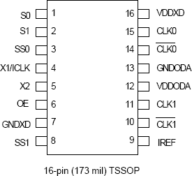
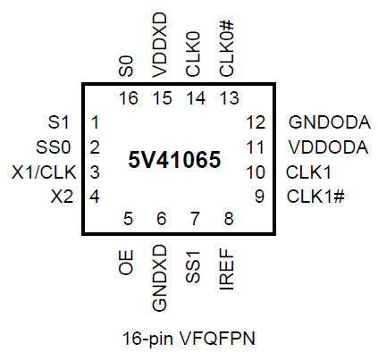
- 16-pin TSSOP and VFQFPN package; small board footprint
- Spread-spectrum capable; reduces EMI
- Outputs can be terminated to LVDS; can drive a wider variety of devices
- 25 MHz, 125 MHz and 200 MHz output frequencies; supports Ethernet applications
- OE control pin; greater system power management
- Spread% and frequency pin selection; no software required to configure device
- Industrial temperature range available; supports demanding embedded applications
- For PCIe Gen3 applications, see the 5V41235
- Cycle-to-cycle jitter < 100 ps
- Output-to-output skew < 50 ps
- PCIe Gen2 phase jitter < 3.0ps RMS
説明
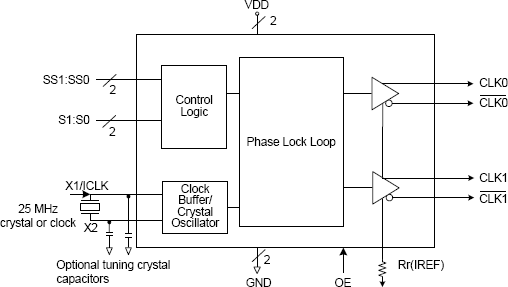
The 5V41065 is a PCIe Gen2 compliant spread spectrum capable clock generator. The device has 2 differential HCSL outputs and can be used in communication or embedded systems to substantially reduce electro-magnetic interference (EMI). The spread amount and output frequency are selectable via select pins. The 5V41065 can also supply 25 MHz, 125 MHz and 200 MHz outputs for applications such as Ethernet.
パラメータ
| 属性 | 値 |
|---|---|
| Diff. Outputs | 2 |
| App Jitter Compliance | PCIe Gen1, PCIe Gen2 |
| Outputs (#) | 2 |
| Output Type | HCSL |
| Output Freq Range (MHz) | 25 - 25, 100 - 100, 125 - 125, 200 - 200 |
| Input Freq (MHz) | 25 - 25 |
| Inputs (#) | 1 |
| Input Type | Crystal, LVCMOS |
| Output Banks (#) | 1 |
| Core Voltage (V) | 3.3 |
| Output Voltage (V) | 3.3 |
| Product Category | PCI Express Clocks |