

| CADモデル: | View CAD Model |
| Pkg. Type: | TSSOP |
| Pkg. Code: | PAG48 |
| Lead Count (#): | 48 |
| Pkg. Dimensions (mm): | 12.5 x 6.1 x 1.0 |
| Pitch (mm): | 0.5 |
| Pb (Lead) Free | Yes |
| Moisture Sensitivity Level (MSL) | 1 |
| ECCN (US) | |
| HTS (US) |
| Pkg. Type | TSSOP |
| Lead Count (#) | 48 |
| Pb (Lead) Free | Yes |
| Carrier Type | Tube |
| Core Voltage (V) | 2.5 |
| Function | Buffer |
| Input Freq (MHz) | 200 |
| Input Type | LVCMOS, LVTTL |
| Inputs (#) | 1 |
| Length (mm) | 12.5 |
| MOQ | 156 |
| Moisture Sensitivity Level (MSL) | 1 |
| Output Banks (#) | 2 |
| Output Freq Range (MHz) | 200 |
| Output Signaling | LVCMOS |
| Output Skew (ps) | 25 |
| Output Type | LVCMOS |
| Output Voltage (V) | 2.5V, 1.8V, 1.5V |
| Outputs (#) | 10 |
| Package Area (mm²) | 76.3 |
| Pb Free Category | e3 Sn |
| Pitch (mm) | 0.5 |
| Pkg. Dimensions (mm) | 12.5 x 6.1 x 1.0 |
| Qty. per Carrier (#) | 39 |
| Qty. per Reel (#) | 0 |
| Requires Terms and Conditions | Does not require acceptance of Terms and Conditions |
| Tape & Reel | No |
| Temp. Range (°C) | -40 to 85°C |
| Thickness (mm) | 1 |
| Width (mm) | 6.1 |
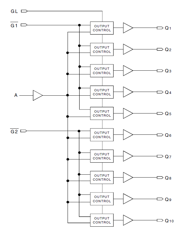
The 5T9070 2.5V single data rate (SDR) clock buffer is a single-ended input to ten single-ended outputs buffer built on advanced metal CMOS technology. The SDR clock buffer fanout from a single input to ten single-ended outputs reduces the loading on the preceding driver and provides an efficient clock distribution network. The 5T9070 has two output banks that can be asynchronously enabled/ disabled. Multiple power and grounds reduce noise.