
特長
- Optimized for 2.5V LVTTL
- Guaranteed Low Skew < 25ps (max)
- Very low duty cycle distortion < 300ps (max)
- High speed propagation delay < 2ns. (max)
- Up to 200MHz operation
- Very low CMOS power levels
- Hot insertable and over-voltage tolerant inputs
- 1:10 fanout buffer
- 2.5V VDD
- Available in TSSOP package
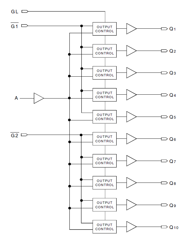
説明
The 5T9070 2.5V single data rate (SDR) clock buffer is a single-ended input to ten single-ended outputs buffer built on advanced metal CMOS technology. The SDR clock buffer fanout from a single input to ten single-ended outputs reduces the loading on the preceding driver and provides an efficient clock distribution network. The 5T9070 has two output banks that can be asynchronously enabled/ disabled. Multiple power and grounds reduce noise.