
| CADモデル: | View CAD Model |
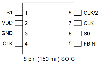
| Pkg. Type: | TSSOP |
| Pkg. Code: | DVG8 |
| Lead Count (#): | 8 |
| Pkg. Dimensions (mm): | 3.0 x 3.0 x 0.97 |
| Pitch (mm): | 0.65 |
| Moisture Sensitivity Level (MSL) | 3 |
| Pb (Lead) Free | Yes |
| ECCN (US) | EAR99 |
| HTS (US) | 8542.39.0090 |
| Lead Count (#) | 8 |
| Carrier Type | Tube |
| Moisture Sensitivity Level (MSL) | 3 |
| Output Skew (ps) | 300 |
| Qty. per Reel (#) | 0 |
| Qty. per Carrier (#) | 96 |
| Core Voltage (V) | 3.3 |
| Input Freq (MHz) | 5 - 55 |
| Multiplication Value | 2, 2.5, 3, 3.333, 4, 5, 5.333, 6, 8 |
| Outputs (#) | 1 |
| Output Freq Range (MHz) | 26 - 110 |
| Output Voltage (V) | 3.3 |
| Package Area (mm²) | 9 |
| Pitch (mm) | 0.65 |
| Pkg. Dimensions (mm) | 3.0 x 3.0 x 0.97 |
| Supply Voltage (V) | 3.3 - 3.3 |
| Pb (Lead) Free | Yes |
| Pb Free Category | e3 Sn |
| Temp. Range (°C) | -40 to 85°C |
| Accepts Spread Spec Input | Yes |
| Advanced Features | Accepts Spread Spec Input |
| Delay Mode | Constant |
| Die Form | No |
| Input Type | LVCMOS |
| Inputs (#) | 1 |
| Length (mm) | 3 |
| MOQ | 288 |
| Output Banks (#) | 1 |
| Output Type | LVCMOS |
| Pkg. Type | TSSOP |
| Product Category | Zero Delay Buffers |
| Requires Terms and Conditions | Does not require acceptance of Terms and Conditions |
| Tape & Reel | No |
| Thickness (mm) | 0.97 |
| Width (mm) | 3 |
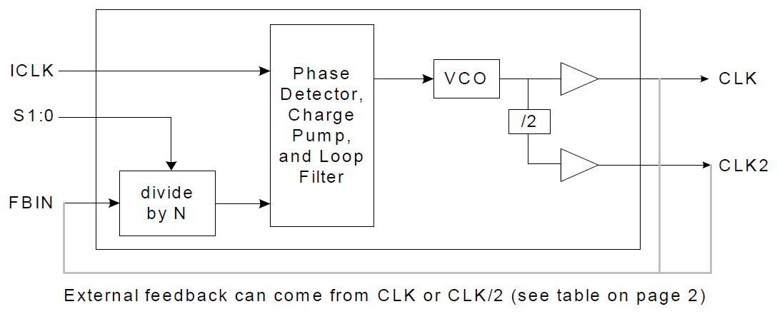
The IDT570 is a high-performance Zero Delay Buffer (ZDB) which integrates IDT's proprietary analog/digital Phase Locked Loop (PLL) techniques. The A version is recommended for 5 V designs and the B version for 3.3 V designs. The chip is part of IDT's ClockBlocks™ family, and was designed as a performance upgrade to meet today's higher speed and lower voltage requirements. The zero delay feature means that the rising edge of the input clock aligns with the rising edges of both output clocks, giving the appearance of no delay through the device. There are two outputs on the chip, one being a low-skew divide by two of the other output. The device incorporates an all-chip power down/tri-state mode that stops the internal PLL and puts both outputs into a high impedance state. The IDT570 is ideal for synchronizing outputs in a large variety of systems, from personal computers to data communications to graphIDT/video. By allowing off-chip feedback paths, the device can eliminate the delay through other devices.