
特長
- 0.5 MICRON CMOS Technology
- Guaranteed low skew < 500ps (max.)
- Very low duty cycle distortion < 1.0ns (max.)
- Very low CMOS power levels
- TTL compatible inputs and outputs
- Inputs can be driven from 3.3V or 5V components
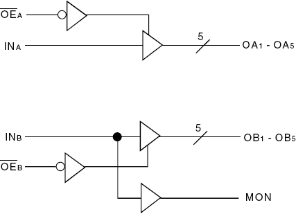
- Two independent output banks with 3-state control
- 1:5 fanout per bank
- "Heartbeat" monitor output
- VCC = 3.3V ± 0.3V
- Available in SSOP, SOIC, and QSOP packages
説明
The FCT3805 is a 3.3 volt, non-inverting clock driver built using advanced dual metal CMOS technology. The device consists of two banks of drivers, each with a 1:5 fanout and its own output enable control. The device has a "heartbeat" monitor for diagnostics and PLL driving. The MON output is identical to all other outputs and complies with the output specifications in this document. The FCT3805 offers low capacitance inputs with hysteresis. The FCT3805 is designed for high speed clock distribution where signal quality and skew are critical. The FCT3805 also allows single point-to-point transmission line driving in applications such as address distribution, where one signal must be distributed to multiple receivers with low skew and high signal quality. For more information on using the FCT3805 with two different input frequencies on bank A and B, please see AN-236.
| Part Number | Status | Samples | Stock | Package | Budgetary Price (USD) | Lead Count (#) | Carrier Type | Moisture Sensitivity Level (MSL) | Qty. per Reel (#) | Qty. per Carrier (#) | Package Area (mm²) | Pitch (mm) | Pkg. Dimensions (mm) | Pb (Lead) Free | Pb Free Category | Temp. Range (°C) | Country of Assembly | Country of Wafer Fabrication |
|---|---|---|---|---|---|---|---|---|---|---|---|---|---|---|---|---|---|---|
| 49FCT3805APYG8 | NRND | N/A | Out of Stock | SSOP | 1ku | $0.69 | 20# | Reel | 1 | 1500# | 0 | 38.2mm² | 0.65mm | 7.2 x 5.3 x 1.73 | Yes | e3 Sn | 0 to 70°C | MALAYSIA | TAIWAN, USA |
| 49FCT3805APYGI8 | NRND | N/A | In Stock | SSOP | 1ku | $0.84 | 20# | Reel | 1 | 1500# | 0 | 38.2mm² | 0.65mm | 7.2 x 5.3 x 1.73 | Yes | e3 Sn | -40 to 85°C | MALAYSIA | TAIWAN, USA |
| 49FCT3805AQG8 | NRND | N/A | In Stock | QSOP | 1ku | $0.69 | 20# | Reel | 1 | 3000# | 0 | 33.1mm² | 0.64mm | 8.7 x 3.8 x 1.47 | Yes | e3 Sn | 0 to 70°C | TAIWAN | TAIWAN, USA |
| 49FCT3805AQGI8 | NRND | N/A | In Stock | QSOP | 1ku | $0.84 | 20# | Reel | 1 | 3000# | 0 | 33.1mm² | 0.64mm | 8.7 x 3.8 x 1.47 | Yes | e3 Sn | -40 to 85°C | TAIWAN | TAIWAN, USA |
| 49FCT3805ASOG8 | Obsolete | N/A | Out of Stock | SOIC | 20# | Reel | 1 | 1000# | 0 | 97.3mm² | 1.27mm | 12.8 x 7.6 x 2.34 | Yes | e3 Sn | 0 to 70°C | |||
| 49FCT3805ASOGI8 | Obsolete | N/A | Out of Stock | SOIC | 20# | Reel | 1 | 1000# | 0 | 97.3mm² | 1.27mm | 12.8 x 7.6 x 2.34 | Yes | e3 Sn | -40 to 85°C | |||
| 49FCT3805PYG | NRND | Available | In Stock | SSOP | 1ku | $0.69 | 20# | Tube | 1 | 0 | 64# | 38.2mm² | 0.65mm | 7.2 x 5.3 x 1.73 | Yes | e3 Sn | 0 to 70°C | MALAYSIA | TAIWAN, USA |
| 49FCT3805PYG8 | NRND | N/A | In Stock | SSOP | 1ku | $0.69 | 20# | Reel | 1 | 1500# | 0 | 38.2mm² | 0.65mm | 7.2 x 5.3 x 1.73 | Yes | e3 Sn | 0 to 70°C | MALAYSIA | TAIWAN, USA |
| 49FCT3805PYGI | NRND | Available | In Stock | SSOP | 1ku | $0.84 | 20# | Tube | 1 | 0 | 64# | 38.2mm² | 0.65mm | 7.2 x 5.3 x 1.73 | Yes | e3 Sn | -40 to 85°C | MALAYSIA | TAIWAN, USA |
| 49FCT3805PYGI8 | NRND | N/A | In Stock | SSOP | 1ku | $0.84 | 20# | Reel | 1 | 1500# | 0 | 38.2mm² | 0.65mm | 7.2 x 5.3 x 1.73 | Yes | e3 Sn | -40 to 85°C | MALAYSIA | TAIWAN, USA |
| 49FCT3805QG | NRND | Available | In Stock | QSOP | 1ku | $0.69 | 20# | Tube | 1 | 0 | 55# | 33.1mm² | 0.64mm | 8.7 x 3.8 x 1.47 | Yes | e3 Sn | 0 to 70°C | TAIWAN | TAIWAN, USA |
| 49FCT3805QG8 | NRND | N/A | In Stock | QSOP | 1ku | $0.69 | 20# | Reel | 1 | 3000# | 0 | 33.1mm² | 0.64mm | 8.7 x 3.8 x 1.47 | Yes | e3 Sn | 0 to 70°C | TAIWAN | TAIWAN, USA |
| 49FCT3805QGI | NRND | Available | In Stock | QSOP | 1ku | $0.84 | 20# | Tube | 1 | 0 | 55# | 33.1mm² | 0.64mm | 8.7 x 3.8 x 1.47 | Yes | e3 Sn | -40 to 85°C | TAIWAN | TAIWAN, USA |
| 49FCT3805QGI8 | NRND | N/A | In Stock | QSOP | 1ku | $0.84 | 20# | Reel | 1 | 3000# | 0 | 33.1mm² | 0.64mm | 8.7 x 3.8 x 1.47 | Yes | e3 Sn | -40 to 85°C | TAIWAN | TAIWAN, USA |
| 49FCT3805SOG | Obsolete | N/A | In Stock | SOIC | 20# | Tube | 1 | 0 | 37# | 97.3mm² | 1.27mm | 12.8 x 7.6 x 2.34 | Yes | e3 Sn | 0 to 70°C | |||
| 49FCT3805SOG8 | Obsolete | N/A | Out of Stock | SOIC | 20# | Reel | 1 | 1000# | 0 | 97.3mm² | 1.27mm | 12.8 x 7.6 x 2.34 | Yes | e3 Sn | 0 to 70°C | |||
| 49FCT3805SOGI | Obsolete | N/A | Out of Stock | SOIC | 20# | Tube | 1 | 0 | 37# | 97.3mm² | 1.27mm | 12.8 x 7.6 x 2.34 | Yes | e3 Sn | -40 to 85°C | |||
| 49FCT3805SOGI8 | Obsolete | N/A | Out of Stock | SOIC | 20# | Reel | 1 | 1000# | 0 | 97.3mm² | 1.27mm | 12.8 x 7.6 x 2.34 | Yes | e3 Sn | -40 to 85°C |
- アプリケーションノート英語PDF 187 KB R31AN0065EU0101 Rev.1.01 2023年11月14日
- アプリケーションノート英語PDF 170 KB 7WDXRDKU4E7E-5-57318 2014年5月13日
- アプリケーションノート英語PDF 495 KB 7WDXRDKU4E7E-5-57312 2014年5月12日
- アプリケーションノート英語PDF 442 KB 7WDXRDKU4E7E-5-57298 2014年5月08日
- 製品変更通知英語PDF 24 KB 7WDXRDKU4E7E-5-41812 2012年11月14日
- アプリケーションノート英語PDF 1.28 MB 7WDXRDKU4E7E-5-32301 2008年10月21日
推奨ドキュメント (1)
データシート (1)
No Results Found.
入力するワードを減らしてみたり、異なるワード、あるいはより一般的なワードを入力してみましょう。
フィルターを適用している場合、フィルターの範囲を見直してみてより広く検索結果が反映される様にしてみましょう。
- ナレッジベースを検索してみましょう。FAQにより、お客様をサポートいたします。
- ルネサスの技術スタッフやコミュニティからのヘルプをサポートフォーラムから受けられます。
- アプリケーションノート英語PDF 187 KB R31AN0065EU0101 Rev.1.01 2023年11月14日
- アプリケーションノート英語PDF 1.99 MB 7WDXRDKU4E7E-5-57242 2022年3月01日
- アプリケーションノート英語PDF 170 KB 7WDXRDKU4E7E-5-57318 2014年5月13日もっと見る (13)
アプリケーションノート、ホワイトペーパー (13)
- 製品変更通知英語PDF 25 KB 7WDXRDKU4E7E-5-63277 2018年9月25日
- 製品変更通知英語PDF 39 KB 7WDXRDKU4E7E-5-63188 2018年8月29日もっと見る (35)
製品通知(PCN、EOLなど) (35)
No Results Found.
入力するワードを減らしてみたり、異なるワード、あるいはより一般的なワードを入力してみましょう。
フィルターを適用している場合、フィルターの範囲を見直してみてより広く検索結果が反映される様にしてみましょう。
- ナレッジベースを検索してみましょう。FAQにより、お客様をサポートいたします。
- ルネサスの技術スタッフやコミュニティからのヘルプをサポートフォーラムから受けられます。
No Results Found.
入力するワードを減らしてみたり、異なるワード、あるいはより一般的なワードを入力してみましょう。
フィルターを適用している場合、フィルターの範囲を見直してみてより広く検索結果が反映される様にしてみましょう。
- ナレッジベースを検索してみましょう。FAQにより、お客様をサポートいたします。
- ルネサスの技術スタッフやコミュニティからのヘルプをサポートフォーラムから受けられます。
No Results Found.
入力するワードを減らしてみたり、異なるワード、あるいはより一般的なワードを入力してみましょう。
フィルターを適用している場合、フィルターの範囲を見直してみてより広く検索結果が反映される様にしてみましょう。
- ナレッジベースを検索してみましょう。FAQにより、お客様をサポートいたします。
- ルネサスの技術スタッフやコミュニティからのヘルプをサポートフォーラムから受けられます。
No Results Found.
入力するワードを減らしてみたり、異なるワード、あるいはより一般的なワードを入力してみましょう。
フィルターを適用している場合、フィルターの範囲を見直してみてより広く検索結果が反映される様にしてみましょう。
- ナレッジベースを検索してみましょう。FAQにより、お客様をサポートいたします。
- ルネサスの技術スタッフやコミュニティからのヘルプをサポートフォーラムから受けられます。
No Results Found.
入力するワードを減らしてみたり、異なるワード、あるいはより一般的なワードを入力してみましょう。
フィルターを適用している場合、フィルターの範囲を見直してみてより広く検索結果が反映される様にしてみましょう。
- ナレッジベースを検索してみましょう。FAQにより、お客様をサポートいたします。
- ルネサスの技術スタッフやコミュニティからのヘルプをサポートフォーラムから受けられます。
No Results Found.
入力するワードを減らしてみたり、異なるワード、あるいはより一般的なワードを入力してみましょう。
フィルターを適用している場合、フィルターの範囲を見直してみてより広く検索結果が反映される様にしてみましょう。
- ナレッジベースを検索してみましょう。FAQにより、お客様をサポートいたします。
- ルネサスの技術スタッフやコミュニティからのヘルプをサポートフォーラムから受けられます。
マーケティング資料 (1)
No Results Found.
入力するワードを減らしてみたり、異なるワード、あるいはより一般的なワードを入力してみましょう。
フィルターを適用している場合、フィルターの範囲を見直してみてより広く検索結果が反映される様にしてみましょう。
- ナレッジベースを検索してみましょう。FAQにより、お客様をサポートいたします。
- ルネサスの技術スタッフやコミュニティからのヘルプをサポートフォーラムから受けられます。
No Results Found.
入力するワードを減らしてみたり、異なるワード、あるいはより一般的なワードを入力してみましょう。
フィルターを適用している場合、フィルターの範囲を見直してみてより広く検索結果が反映される様にしてみましょう。
- ナレッジベースを検索してみましょう。FAQにより、お客様をサポートいたします。
- ルネサスの技術スタッフやコミュニティからのヘルプをサポートフォーラムから受けられます。
フィルター
適用されたフィルター
ソフトウェア/ツール
タイプでの検索
プロバイダでの検索
サンプルコード
アプリケーションでの検索
ファンクションでの検索
コンパイラでの検索
IDE に関するフィルタリング
シミュレーションモデル
Partner Solutions
No Results Found.
入力するワードを減らしてみたり、異なるワード、あるいはより一般的なワードを入力してみましょう。
フィルターを適用している場合、フィルターの範囲を見直してみてより広く検索結果が反映される様にしてみましょう。
- ナレッジベースを検索してみましょう。FAQにより、お客様をサポートいたします。
- ルネサスの技術スタッフやコミュニティからのヘルプをサポートフォーラムから受けられます。
No Results Found.
入力するワードを減らしてみたり、異なるワード、あるいはより一般的なワードを入力してみましょう。
フィルターを適用している場合、フィルターの範囲を見直してみてより広く検索結果が反映される様にしてみましょう。
- ナレッジベースを検索してみましょう。FAQにより、お客様をサポートいたします。
- ルネサスの技術スタッフやコミュニティからのヘルプをサポートフォーラムから受けられます。
No Results Found.
入力するワードを減らしてみたり、異なるワード、あるいはより一般的なワードを入力してみましょう。
フィルターを適用している場合、フィルターの範囲を見直してみてより広く検索結果が反映される様にしてみましょう。
- ナレッジベースを検索してみましょう。FAQにより、お客様をサポートいたします。
- ルネサスの技術スタッフやコミュニティからのヘルプをサポートフォーラムから受けられます。
シミュレーションモデル (2)
No Results Found.
入力するワードを減らしてみたり、異なるワード、あるいはより一般的なワードを入力してみましょう。
フィルターを適用している場合、フィルターの範囲を見直してみてより広く検索結果が反映される様にしてみましょう。
- ナレッジベースを検索してみましょう。FAQにより、お客様をサポートいたします。
- ルネサスの技術スタッフやコミュニティからのヘルプをサポートフォーラムから受けられます。


