Features
- Gen IV technology
- JEDEC-qualified GaN technology
- Dynamic RDS(on)eff production tested
- Robust design, defined by
- Wide gate safety margin
- Transient over-voltage capability
- Very low QRR
- Reduced crossover loss
- Achieves increased efficiency in both hard- and soft-switched circuits
- Increased power density
- Reduced system size and weight
- Overall lower system cost
- Easy to drive with commonly-used gate drivers
- GSD pin layout improves high speed design
- RoHS-compliant and Halogen-free packaging
Description
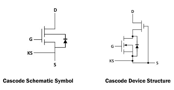
The TP65H070G4LSGB 650V 72mΩ Gallium Nitride (GaN) FET is a normally-off device built using our Gen IV platform. It combines state-of-the-art high voltage GaN HEMT and low voltage silicon MOSFET technologies—offering superior reliability and performance.
Renesas' GaN power products offer improved efficiency over silicon through lower gate charge, lower crossover loss, and smaller reverse recovery charge.
The TP65H070G4LSGB is offered in an industry-standard PQFN88 with a common source package configuration.
Applications
- Datacom
- Broad industrial
- PV inverter
- Servo motor
- Consumer
- Computing
| Part Number | Status | Samples | Stock | Package | Carrier Type | Moisture Sensitivity Level (MSL) | Mounting Type | Temp. Range (°C) |
|---|---|---|---|---|---|---|---|---|
| TP65H070G4LSGB | NRND | N/A | Out of Stock | PQFN88 | Tape & Reel | 3 | Surface Mount | -55 to +150°C |
Filters
Applied Filters
- White PaperPDF 1.9 MB R16WP0012EU0100 Rev.1.00 Dec 19, 2025D-Mode GaN combines the best of both GaN and Silicon and is ideal for high-voltage applications with high-speed, high-voltage GaN switching, robust 4V threshold gate compatible with standard gate drivers, and a range of standard package offerings not available with other GaN technologies.
- Technical BriefPDF 992 KB R16TB0004EU0100 Rev.1.00 Dec 02, 2025
- DatasheetTP65H070G4LSGBEA DatasheetRECOMMENDEDPDF 818 KB R07DS1619EU0200 Rev.2.00 Nov 25, 2025The TP65H070G4LSGBEA 650V, 72mΩ Gallium Nitride (GaN) FET is a normally-off device combining a high-voltage D-mode GaN HEMT and low-voltage silicon MOSFET. It offers enhanced noise immunity with a 4V threshold voltage with no negative gate drive required. The Renesas Gen IV SuperGaN® platform uses advanced epi to improve efficiency over silicon via lower gate charge, output capacitance, crossover loss, and reverse recovery charge.
- Application NotePDF 372 KB Dec 11, 2024AI-generated Summary: GaN power switches require careful PCB layout and probing techniques to fully utilize their fast switching capabilities. Minimizing parasitic inductances and capacitances in the power and gate drive loops reduces ringing and ensures stable operation. A large ground plane, close placement of power components, and short, wide traces in the gate drive circuit improve performance. Accurate probing demands short ground leads and direct probe placement to avoid measurement artifacts. Avoid adding parasitics during probing by using floating oscilloscopes and minimizing wire lengths. The document also highlights the importance of proper decoupling and grounding strategies for high-frequency switching circuits.
- Application NotePDF 3.39 MB Jan 17, 2024AI-generated Summary: The document details tape and reel packaging specifications for various PQFN packages by Renesas Electronics, including GEN III and GEN IV 8x8mm and 5x6mm sizes. It covers product orientation, carrier tape dimensions, reel sizes, box sizes, package PODs, laser marking samples, and shipping box information. The GEN III 8x8mm PQFN tape and reel includes 500 pieces per reel, with leader and trailer empty pocket lengths specified. Carrier tape dimensions follow EIA 481 standards with precise sprocket hole tolerances. Reel size is standardized at 178mm diameter. The document also includes detailed packaging and shipping information for TO-220, TO-247, and TOLL tape and reel formats.
- Application NotePDF 676 KB Jan 02, 2023AI-generated Summary: The document evaluates the DGD2304 high voltage, high speed half-bridge gate driver as a cost-effective solution for low- to mid-power GaN FET applications. It highlights the DGD2304’s compatibility with TTL/CMOS logic, 600 V bootstrap operation, internal deadtime to prevent shoot-through, and extended temperature range. The evaluation uses Transphorm’s 1200 W Buck/Boost kit and compares the DGD2304 to the higher-cost Si8230 driver. The document includes schematics and PCB layouts for daughter cards integrating the DGD2304, emphasizing its suitability for applications where isolation is unnecessary, such as power adapters and chargers. Design files like BOM, schematics, and Gerber files are bundled for reference.
- Application NotePDF 1.26 MB Apr 07, 2022AI-generated Summary: Recommendations focus on lead-free second-level soldering for PQFN88, PQFN56, and TO-263 packages using vapor phase reflow. Key points include PCB footprint design to ensure optimal thermal and electrical performance, solder pad surface finish selection favoring Electroless Ni/Immersion Au (ENIG) for superior solder wetting, and solder stencil specifications with preferred thickness around 127µm. Vias in drain or source pads improve thermal conduction. Detailed stencil aperture dimensions and solder mask openings support self-alignment during reflow soldering. The document guides on solder paste printing and reflow parameters to achieve reliable assembly.
- GuidePDF 225 KB Jul 14, 2017Related Files:
- DatasheetTP65H070G4LSGBEA DatasheetRECOMMENDEDPDF 818 KB R07DS1619EU0200 Rev.2.00 Nov 25, 2025The TP65H070G4LSGBEA 650V, 72mΩ Gallium Nitride (GaN) FET is a normally-off device combining a high-voltage D-mode GaN HEMT and low-voltage silicon MOSFET. It offers enhanced noise immunity with a 4V threshold voltage with no negative gate drive required. The Renesas Gen IV SuperGaN® platform uses advanced epi to improve efficiency over silicon via lower gate charge, output capacitance, crossover loss, and reverse recovery charge.
Recommended Documents (2)
- DatasheetTP65H070G4LSGBEA DatasheetRECOMMENDEDPDF 818 KB R07DS1619EU0200 Rev.2.00 Nov 25, 2025The TP65H070G4LSGBEA 650V, 72mΩ Gallium Nitride (GaN) FET is a normally-off device combining a high-voltage D-mode GaN HEMT and low-voltage silicon MOSFET. It offers enhanced noise immunity with a 4V threshold voltage with no negative gate drive required. The Renesas Gen IV SuperGaN® platform uses advanced epi to improve efficiency over silicon via lower gate charge, output capacitance, crossover loss, and reverse recovery charge.
Datasheets (2)
- GuidePDF 225 KB Jul 14, 2017Related Files:
- GuidePDF 273 KB Jul 11, 2017Related Files:View More (6)
Manuals & Guides (6)
- White PaperPDF 1.9 MB R16WP0012EU0100 Rev.1.00 Dec 19, 2025D-Mode GaN combines the best of both GaN and Silicon and is ideal for high-voltage applications with high-speed, high-voltage GaN switching, robust 4V threshold gate compatible with standard gate drivers, and a range of standard package offerings not available with other GaN technologies.
- Application NotePDF 372 KB Dec 11, 2024AI-generated Summary: GaN power switches require careful PCB layout and probing techniques to fully utilize their fast switching capabilities. Minimizing parasitic inductances and capacitances in the power and gate drive loops reduces ringing and ensures stable operation. A large ground plane, close placement of power components, and short, wide traces in the gate drive circuit improve performance. Accurate probing demands short ground leads and direct probe placement to avoid measurement artifacts. Avoid adding parasitics during probing by using floating oscilloscopes and minimizing wire lengths. The document also highlights the importance of proper decoupling and grounding strategies for high-frequency switching circuits.
- Application NotePDF 3.39 MB Jan 17, 2024AI-generated Summary: The document details tape and reel packaging specifications for various PQFN packages by Renesas Electronics, including GEN III and GEN IV 8x8mm and 5x6mm sizes. It covers product orientation, carrier tape dimensions, reel sizes, box sizes, package PODs, laser marking samples, and shipping box information. The GEN III 8x8mm PQFN tape and reel includes 500 pieces per reel, with leader and trailer empty pocket lengths specified. Carrier tape dimensions follow EIA 481 standards with precise sprocket hole tolerances. Reel size is standardized at 178mm diameter. The document also includes detailed packaging and shipping information for TO-220, TO-247, and TOLL tape and reel formats.
- Application NotePDF 676 KB Jan 02, 2023AI-generated Summary: The document evaluates the DGD2304 high voltage, high speed half-bridge gate driver as a cost-effective solution for low- to mid-power GaN FET applications. It highlights the DGD2304’s compatibility with TTL/CMOS logic, 600 V bootstrap operation, internal deadtime to prevent shoot-through, and extended temperature range. The evaluation uses Transphorm’s 1200 W Buck/Boost kit and compares the DGD2304 to the higher-cost Si8230 driver. The document includes schematics and PCB layouts for daughter cards integrating the DGD2304, emphasizing its suitability for applications where isolation is unnecessary, such as power adapters and chargers. Design files like BOM, schematics, and Gerber files are bundled for reference.
- Application NotePDF 1.26 MB Apr 07, 2022AI-generated Summary: Recommendations focus on lead-free second-level soldering for PQFN88, PQFN56, and TO-263 packages using vapor phase reflow. Key points include PCB footprint design to ensure optimal thermal and electrical performance, solder pad surface finish selection favoring Electroless Ni/Immersion Au (ENIG) for superior solder wetting, and solder stencil specifications with preferred thickness around 127µm. Vias in drain or source pads improve thermal conduction. Detailed stencil aperture dimensions and solder mask openings support self-alignment during reflow soldering. The document guides on solder paste printing and reflow parameters to achieve reliable assembly.
Application Notes & White Papers (5)
No Results Found.
Make sure all keywords are spelled correctly.
Try fewer, different, or more general terms to vary your search.
If you have filters applied, consider deselecting some to broaden your results.
- Search our extensive knowledgebase, designed to help customers with their FAQs.
- Get help from our expert Renesas technical staff and community on our support forums.
No Results Found.
Make sure all keywords are spelled correctly.
Try fewer, different, or more general terms to vary your search.
If you have filters applied, consider deselecting some to broaden your results.
- Search our extensive knowledgebase, designed to help customers with their FAQs.
- Get help from our expert Renesas technical staff and community on our support forums.
No Results Found.
Make sure all keywords are spelled correctly.
Try fewer, different, or more general terms to vary your search.
If you have filters applied, consider deselecting some to broaden your results.
- Search our extensive knowledgebase, designed to help customers with their FAQs.
- Get help from our expert Renesas technical staff and community on our support forums.
- PCB Design FilesZIP 2.7 MB Jul 11, 2017Related Files:
Schematics & Design Files (1)
No Results Found.
Make sure all keywords are spelled correctly.
Try fewer, different, or more general terms to vary your search.
If you have filters applied, consider deselecting some to broaden your results.
- Search our extensive knowledgebase, designed to help customers with their FAQs.
- Get help from our expert Renesas technical staff and community on our support forums.
No Results Found.
Make sure all keywords are spelled correctly.
Try fewer, different, or more general terms to vary your search.
If you have filters applied, consider deselecting some to broaden your results.
- Search our extensive knowledgebase, designed to help customers with their FAQs.
- Get help from our expert Renesas technical staff and community on our support forums.
No Results Found.
Make sure all keywords are spelled correctly.
Try fewer, different, or more general terms to vary your search.
If you have filters applied, consider deselecting some to broaden your results.
- Search our extensive knowledgebase, designed to help customers with their FAQs.
- Get help from our expert Renesas technical staff and community on our support forums.
No Results Found.
Make sure all keywords are spelled correctly.
Try fewer, different, or more general terms to vary your search.
If you have filters applied, consider deselecting some to broaden your results.
- Search our extensive knowledgebase, designed to help customers with their FAQs.
- Get help from our expert Renesas technical staff and community on our support forums.
- Technical BriefPDF 992 KB R16TB0004EU0100 Rev.1.00 Dec 02, 2025
Other (3)
No Results Found.
Make sure all keywords are spelled correctly.
Try fewer, different, or more general terms to vary your search.
If you have filters applied, consider deselecting some to broaden your results.
- Search our extensive knowledgebase, designed to help customers with their FAQs.
- Get help from our expert Renesas technical staff and community on our support forums.
No Results Found.
Make sure all keywords are spelled correctly.
Try fewer, different, or more general terms to vary your search.
If you have filters applied, consider deselecting some to broaden your results.
- Search our extensive knowledgebase, designed to help customers with their FAQs.
- Get help from our expert Renesas technical staff and community on our support forums.
Filters
Applied Filters
Software & Tools
Filter by Type
Filter by Provider
Sample Code
Filter by Application
Filter by Function
Filter by Compiler
Filter by IDE
Simulation Models
Partner Solutions
- PCB Design FilesZIP 2.7 MB Jul 11, 2017Related Files:
No Results Found.
Make sure all keywords are spelled correctly.
Try fewer, different, or more general terms to vary your search.
If you have filters applied, consider deselecting some to broaden your results.
- Search our extensive knowledgebase, designed to help customers with their FAQs.
- Get help from our expert Renesas technical staff and community on our support forums.
- PCB Design FilesZIP 2.7 MB Jul 11, 2017Related Files:
Software & Tools (1)
No Results Found.
Make sure all keywords are spelled correctly.
Try fewer, different, or more general terms to vary your search.
If you have filters applied, consider deselecting some to broaden your results.
- Search our extensive knowledgebase, designed to help customers with their FAQs.
- Get help from our expert Renesas technical staff and community on our support forums.
Simulation Models (1)
No Results Found.
Make sure all keywords are spelled correctly.
Try fewer, different, or more general terms to vary your search.
If you have filters applied, consider deselecting some to broaden your results.
- Search our extensive knowledgebase, designed to help customers with their FAQs.
- Get help from our expert Renesas technical staff and community on our support forums.
Support Communities
-
Footprint for GaN, PQFN88 with KS port
Hi, I'd like to use the TP65H070G4LSGBEA for next development item. I requested to create the footprint from REL web. However, it has not reference document, REL could not create it.Can I get it from you? BR, ACGUY
Jan 6, 2026 -
Inquiry on Longevity and Comparison of SuperGaN FETs
Dear Team, I would like to inquire about the general longevity of our SuperGaN FETs. Specifically, for the TP65H070G4LSG and TP65H070G4LSGB, could you please clarify the differences between these two parts, apart from the pinout (PQFN88 package)? Which part would be more recommended for use in new projects? Additionally, do ...
Nov 22, 2024 -
TP65H070LDG
Hi, I use in our new project TP65H070LDG Is it active part? Best Regards Boris Voznesensky
Nov 18, 2024