Features
- Ultra-low phase noise synthesizer: Jitter below 18fs RMS from 12kHz to 20MHz with a 4MHz high pass filter (HPF)
- Independent synchronization domains: Three independent low phase noise synchronization domains
- Frequency domains: Four independent low phase noise frequency domains
- Protocol support: Compatible with JESD204B/C standards
- Time synchronization features: Equipped with a time-to-digital converter (TDC), time of day (TOD) counter, and precision time protocol (PTP) clocks
- Clock outputs: 12 clock outputs with independent integer dividers
- 8 outputs using LVDS, HCSL (AC-LVPECL), or CML
- 4 outputs using LVDS, HCSL (AC-LVPECL), or LVCMOS
- Output frequency range
- CML: DC to 2.5GHz
- LVDS or HCSL: DC to 1GHz
- LVCMOS: DC to 250MHz
- Input clock specifications
- Clock inputs: Four differential or single-ended clock inputs
- Voltage tolerance: Clock inputs tolerate 1.8V input when the device is powered off, sinking less than 1mA
- Input frequency range: CLKIN input frequency from DC to 1GHz
- Time sync TDC: Supports 1 pulse per second (1PPS) and pulse per two seconds (PP2S) inputs
- Digital phase-locked loops (DPLLs)
- Comply with ITU-T G.8262 and G.8262.1 standards
- Input-to-output phase variation ≤ 100ps
- Digitally controlled oscillator (DCO): Frequency resolution < 10^-13
- Operating voltage: Functions on a 1.8V supply
- Packaging: Compact 9mm x 9mm size in a 100-pin BGA

Description
The RC38312 is an ultra-low phase noise radio synchronizer, multi-frequency clock synthesizer, and digitally controlled oscillator (DCO). It delivers exceptional performance for 5G radio units (RU), distribution units (DU), and network switches and routers. Its capability to output clocks with ultra-low in-band phase noise and significantly reduced spurious levels enhances the reliability and efficiency of 4G and 5G RF transceivers. The device offers the most margin on reference clock jitter, with up to three synchronization domains and four frequency domains, allowing designers to simplify their overall PCB design and providing a single timing solution supporting both synchronization via CPRI or eCPRI and RF clock generation. It offers low power dissipation and a smaller area while still achieving ultra-low jitter, and maintains ultra-low phase coherence essential for 5G and 5G-A BTS radio unit designs. The RC38312 provides flexibility by allowing locking to external reference clocks or free-running crystals/oscillators and features hitless reference switching to ensure uninterrupted service even when switching between redundant timing sources, making it an ideal choice for ensuring robust, precise timing across telecommunication applications.
Parameters
| Attributes | Value |
|---|---|
| Outputs (#) | 12 |
| Output Type | HCSL, LVCMOS, LVDS |
| Output Freq Range (MHz) | 5.0E-7 - 1000 |
| Input Freq (MHz) | 5.0E-7 - 1000 |
| Inputs (#) | 8 |
| Input Type | CML, Crystal, HCSL, LVCMOS, LVDS, LVPECL |
| Output Banks (#) | 12 |
| Core Voltage (V) | 1.8V, 3.3V |
| Output Voltage (V) | 1.8 |
| Product Category | FemtoClock 3 |
Package Options
| Pkg. Type | Pkg. Dimensions (mm) | Lead Count (#) | Pitch (mm) |
|---|---|---|---|
| CABGA | 9.0 x 9.0 x 1.1 | 100 | 0.8 |
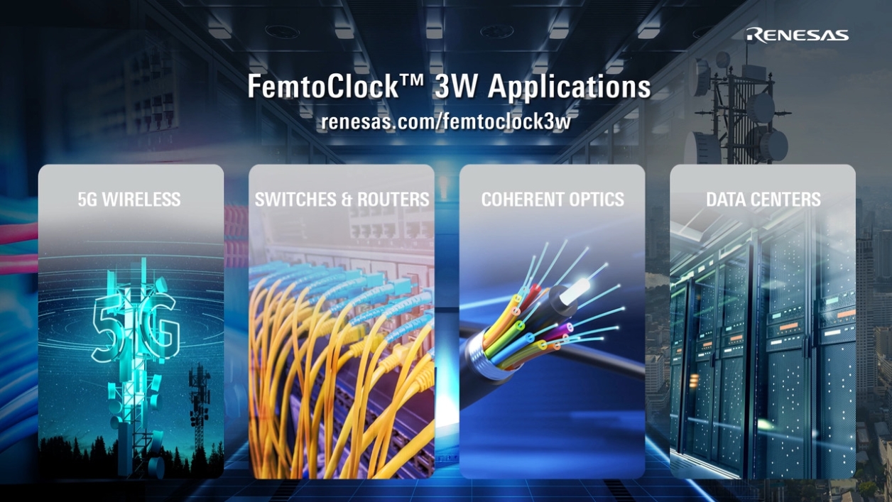
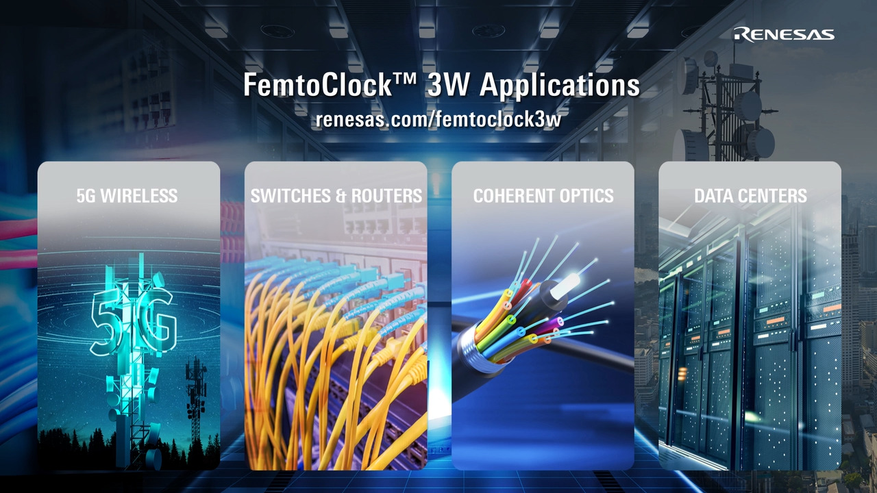
Applications
- 5G radio units (RU)
- 5G distribution units (DU), switches, and routers
- Reference clock for 112Gbps and 224Gbps SerDes
- High-performance DCO for precision time protocol (PTP) based clocks
- Datacenter switch, accelerator card, AI interconnect
Renesas Boards & Kits
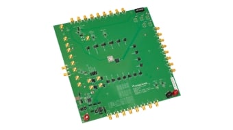
FemtoClock 3 Wireless Ultra-Low Phase Noise Synchronizer and Jitter Attenuator Evaluation Kit
This RC38312A evaluation kit is used to evaluate the RC38312 FemtoClock™ 3 ultra-low phase noise radio synchronizer, multi-frequency clock synthesizer. The RC38312/RC38112 is an ultra-low phase noise radio synchronizer, multi-frequency clock synthesizer, and digitally controlled oscillator... Read More
Knowledge Base
-
Do you have a reference design for the RC38312?
Yes, we have a reference design based on the BGA100 device. See attached schematic.
Oct 8, 2024 -
How can I achieve the best performance for the FemtoClock 3 Wireless in regards to phase noise with the lowest crosstalk.
FemtoClock 3 (FC3) and FemtoClock 3 Wireless (FC3W) devices are a family of telecom integrated circuits that are low-phase noise jitter attenuators. These include the RC32312 and RC32308 (FC3) or the RC38108, RC38208, RC38112 and RC38312 (FC3W). There are also FC3 devices that are only frequency clock synthesizers, such ...
Oct 8, 2024

Support Communities


