Features
- Accepts 3.3V/5V logic level PWM inputs
- 7.2A source and 5.3A sink driver for GaN/MOSFET
- Separately adjusts turn-on and turn-off speed
- Supports positive and negative PWM or EN input logic
- Fast propagation delay: 5ns typical delay
- 7ns minimum input pulse width
- 4ns typical rise and fall time
- 5V power supply
- VDD undervoltage lockout (UVLO) and over-temperature protection (OTP)
- Small package with low parasitic inductance, supporting up to 30MHz switching frequency applications
- Low power consumption
- 2mm × 2mm SCTDFN package

RRP63175 Low-Side Driver Typical Application
Description
The RRP63175 is a high-frequency single low-side driver for E-mode GaN and logic-level MOSFET. It functions as a 5V, 7.2A source, and a 5.3A sink while supporting 3.3V and 5V logic-level PWM input signals.
With a typical propagation delay of just 5ns, the RRP63175 is ideal for high-frequency switching applications. It is capable of operating at frequencies of up to 30MHz.
Parameters
| Attributes | Value |
|---|---|
| Drivers (#) | 1 |
| Input Voltage (Max) (V) | 6 |
| Peak Output Current IPK (A) | 7.2 |
| Rise Time (μs) | 0.004 |
| Fall Time | 0.004 |
| Turn On Delay (ns) | 5 |
| Turn Off Delay (ns) | 5 |
| IS (mA) | 5.9 |
| Input Supply Range (V) | 5.5 |
| Output Signal Range | 0 - 5.5 |
| Input Signal Range | 0 - 3.3/5 |
| Simulation Model Available | iSim |
Package Options
| Pkg. Type | Pkg. Dimensions (mm) | Lead Count (#) | Pitch (mm) |
|---|---|---|---|
| SCDFN | 2.0 x 2.0 x 0.75 | 6 | 0.7 |
Applications
- GaN/MOSFET synchronous rectifier
- Power modules
- DC/DC converter
Renesas Boards & Kits
RTKP63175
Active
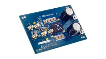
RPP63175 Low-Side Driver Evaluation Board with GaN/MOSFET in Boost System
The RRP63175 evaluation boards (RTKP63175DE00000BC and RTKP63175DE00010BC) enable a rapid and thorough evaluation of the RRP63175, a single low-side driver capable of driving 7.2A source and 5.3A sink currents. These boards are designed to efficiently drive the gates of either GaN FETs... Read More
Recommended Documents:

Support Communities
Get quick technical support online from Renesas Engineering Community technical staff.

Knowledge Base
Browse our knowledge base for helpful articles, FAQs, and other useful resources.

