Features
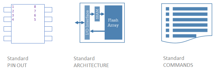
- Universally compatible pinout and command set
- Standard block architecture
- Supports Dual I/O, Quad I/O operation
Description
The AT25SF641 is a member of our standard class code and data storage solutions designed for 3V systems in which program code is shadowed from Flash memory into embedded or external RAM for execution.
The architecture includes erase block sizes that are optimized to meet the needs of today's code and data storage applications and three security register pages for unique device serialization, system-level Electronic Serial Number (ESN) storage, locked key storage, etc.
| Part Number | Status | Samples | Stock | Package | Carrier Type |
|---|---|---|---|---|---|
| AT25SF641-DWF | NRND | N/A | Out of Stock | See Wafer-Die Solution Menu | |
| AT25SF641-MHB-T | NRND | N/A | Out of Stock | DFN | Tape & Reel |
| AT25SF641-SUB-T | NRND | N/A | Out of Stock | SOIC-W | Tape & Reel |
Filters
Applied Filters
- Application NotePDF 884 KB R10AN0038EU0100 Rev.1.00 Mar 10, 2026This application note discusses endurance and data retention in NOR Flash memory products. It describes the structure and operation of the NOR Flash transistor, the mechanisms of NOR Flash device failure and oxide degradation which limit endurance and data retention. It explains JEDEC-based test procedures for certifying endurance and data retention specifications and ways to mitigate limitations. The first part of this document and the appendix provide background for understanding the issue. The later sections describe practical scenarios of interest to most customers.
- Application NotePDF 695 KB AN503 Sep 05, 2025Explores thermal resistance in integrated circuits (ICs) and details its role in managing heat from power consumption to ensure reliable operation. Proper thermal management enhances IC performance and longevity. Thermal resistance, measured in °C/W, quantifies heat flow resistance from the silicon die to the environment or PCB, with key types including junction-to-case (θJC), case-to-ambient (θCA), junction-to-ambient (θJA), and junction-to-board (θJB).
- Application NotePDF 2.62 MB AN500 Feb 13, 2024AI-generated Summary: NOR Flash memory requires an erase operation before programming, which occurs in three phases: Pre-Program, Erase, and Recovery. The erase process affects entire blocks simultaneously, not byte-by-byte. Memory cells use floating gate MOSFETs to store data, organized into arrays of rows (Word-Lines) and columns (Bit-Lines). Physical Blocks contain multiple Logical Blocks and share common p-wells and Bit-Lines, impacting operation. Smaller Logical Blocks enable improved erase performance through parallelization. Understanding these processes and potential interruptions is crucial for designing reliable systems.
- Application NotePDF 710 KB AN502 Jan 24, 2024AI-generated Summary: Renesas NOR flash devices require decoupling capacitors close to VCC and GND pins to stabilize voltage, typically 1 μF with an optional 100 nF capacitor. Pull-up resistors are recommended on CS#, WP#/IO2, and HOLD#/IO3 pins to ensure proper signal states and facilitate debugging. Signal routing should minimize trace length and maintain a solid ground plane for high-speed signals. Power supply must rise monotonically during power-up. Basic system bring-up involves verifying installation, voltage levels, and SPI communication using manufacturer/device ID commands. Software drivers depend on host MCU architecture; Renesas offers example drivers and support. Correct erase/program sequences include write-enable, erase/program commands, and status checks. Tools for programming include flash loader plug-ins and debug probes. Switching from single to quad-SPI involves setting the quad-enable bit, changing pin functions. Dummy cycles introduce necessary wait times during read commands to accommodate latency.
- GuidePDF 790 KB SPI_NOR_Flash_Product_Guide_PBFLASH03102022rev-C Jun 16, 2023
- DocumentPDF 1 MB R10DS0315EU0000 Rev.0.00 Jun 28, 2022
- Application NotePDF 794 KB May 12, 2022AI-generated Summary: Renesas NOR flash devices implement multiple protection methods to safeguard memory arrays, status registers, flash states, and resets from accidental or intentional modifications. Protection types include hardware-based write protection via the WP pin and software-based protection through commands controlling status registers and memory blocks. Memory array protection schemes include individual block protection, allowing sector-level lock/unlock, and memory edge protection, which protects contiguous regions aligned to memory edges. Status register protection indirectly secures memory by blocking changes to protection states. Detailed command sets and register bits configure these protections, ensuring robust flash memory integrity.
- Application NotePDF 663 KB Oct 18, 2021AI-generated Summary: Proper power-up and power-down sequencing is critical for NOR Flash memory operation to ensure reliable system performance. The power supply voltage must ramp up monotonically without dips, reaching the minimum operational voltage within specified timing to avoid corrupted initialization. Reset methods, including hardware and JEDEC resets, help ensure the device starts from a known state. Brown-out conditions and power cycling require careful handling to prevent data corruption and ensure stable operation. The document covers power sequencing, reset types, brown-out recovery, power-down, and power-saving modes, providing essential guidelines for system engineers and application developers.
- Technical UpdatePDF 399 KB Aug 07, 2020Potential side effects of excessive CS toggling are examined for Renesas AT25SF641 and AT25QF641 Flash devices, with findings applicable exclusively to these products. This document offers design tips to extend device life under high-stress conditions, such as frequent CS toggles.
- Application NotePDF 313 KB Jul 17, 2020AI-generated Summary: PCB design for Adesto memory devices requires careful placement of decoupling capacitors close to VCC and GND pins to minimize voltage fluctuations caused by parasitic inductance and capacitance in PCB traces. Proper capacitor selection and placement reduce signal integrity issues, EMI, and noise. Design guidelines vary by package type (SOIC, UDFN, WLCSP, BGA) and PCB layer count. Signal routing rules ensure reliable data and control signals. Special cases include parallel devices, reset signal handling, and test point integration. The document provides detailed layout recommendations for each package type to optimize device performance and reliability.
Recommended Documents (1)
Datasheets (1)
- GuidePDF 790 KB SPI_NOR_Flash_Product_Guide_PBFLASH03102022rev-C Jun 16, 2023
Manuals & Guides (1)
- Application NotePDF 884 KB R10AN0038EU0100 Rev.1.00 Mar 10, 2026This application note discusses endurance and data retention in NOR Flash memory products. It describes the structure and operation of the NOR Flash transistor, the mechanisms of NOR Flash device failure and oxide degradation which limit endurance and data retention. It explains JEDEC-based test procedures for certifying endurance and data retention specifications and ways to mitigate limitations. The first part of this document and the appendix provide background for understanding the issue. The later sections describe practical scenarios of interest to most customers.
- Application NotePDF 695 KB AN503 Sep 05, 2025Explores thermal resistance in integrated circuits (ICs) and details its role in managing heat from power consumption to ensure reliable operation. Proper thermal management enhances IC performance and longevity. Thermal resistance, measured in °C/W, quantifies heat flow resistance from the silicon die to the environment or PCB, with key types including junction-to-case (θJC), case-to-ambient (θCA), junction-to-ambient (θJA), and junction-to-board (θJB).
- Application NotePDF 2.62 MB AN500 Feb 13, 2024AI-generated Summary: NOR Flash memory requires an erase operation before programming, which occurs in three phases: Pre-Program, Erase, and Recovery. The erase process affects entire blocks simultaneously, not byte-by-byte. Memory cells use floating gate MOSFETs to store data, organized into arrays of rows (Word-Lines) and columns (Bit-Lines). Physical Blocks contain multiple Logical Blocks and share common p-wells and Bit-Lines, impacting operation. Smaller Logical Blocks enable improved erase performance through parallelization. Understanding these processes and potential interruptions is crucial for designing reliable systems.
- Application NotePDF 710 KB AN502 Jan 24, 2024AI-generated Summary: Renesas NOR flash devices require decoupling capacitors close to VCC and GND pins to stabilize voltage, typically 1 μF with an optional 100 nF capacitor. Pull-up resistors are recommended on CS#, WP#/IO2, and HOLD#/IO3 pins to ensure proper signal states and facilitate debugging. Signal routing should minimize trace length and maintain a solid ground plane for high-speed signals. Power supply must rise monotonically during power-up. Basic system bring-up involves verifying installation, voltage levels, and SPI communication using manufacturer/device ID commands. Software drivers depend on host MCU architecture; Renesas offers example drivers and support. Correct erase/program sequences include write-enable, erase/program commands, and status checks. Tools for programming include flash loader plug-ins and debug probes. Switching from single to quad-SPI involves setting the quad-enable bit, changing pin functions. Dummy cycles introduce necessary wait times during read commands to accommodate latency.
Application Notes & White Papers (8)
- Product Change NoticePDF 528 KB Jun 26, 2020
Product Notices (PCN, EOL, etc) (3)
- Technical UpdatePDF 399 KB Aug 07, 2020Potential side effects of excessive CS toggling are examined for Renesas AT25SF641 and AT25QF641 Flash devices, with findings applicable exclusively to these products. This document offers design tips to extend device life under high-stress conditions, such as frequent CS toggles.
Errata & Technical Updates (1)
No Results Found.
Make sure all keywords are spelled correctly.
Try fewer, different, or more general terms to vary your search.
If you have filters applied, consider deselecting some to broaden your results.
- Search our extensive knowledgebase, designed to help customers with their FAQs.
- Get help from our expert Renesas technical staff and community on our support forums.
No Results Found.
Make sure all keywords are spelled correctly.
Try fewer, different, or more general terms to vary your search.
If you have filters applied, consider deselecting some to broaden your results.
- Search our extensive knowledgebase, designed to help customers with their FAQs.
- Get help from our expert Renesas technical staff and community on our support forums.
No Results Found.
Make sure all keywords are spelled correctly.
Try fewer, different, or more general terms to vary your search.
If you have filters applied, consider deselecting some to broaden your results.
- Search our extensive knowledgebase, designed to help customers with their FAQs.
- Get help from our expert Renesas technical staff and community on our support forums.
No Results Found.
Make sure all keywords are spelled correctly.
Try fewer, different, or more general terms to vary your search.
If you have filters applied, consider deselecting some to broaden your results.
- Search our extensive knowledgebase, designed to help customers with their FAQs.
- Get help from our expert Renesas technical staff and community on our support forums.
No Results Found.
Make sure all keywords are spelled correctly.
Try fewer, different, or more general terms to vary your search.
If you have filters applied, consider deselecting some to broaden your results.
- Search our extensive knowledgebase, designed to help customers with their FAQs.
- Get help from our expert Renesas technical staff and community on our support forums.
Marketing Collateral (1)
- DocumentPDF 1 MB R10DS0315EU0000 Rev.0.00 Jun 28, 2022
Other (2)
No Results Found.
Make sure all keywords are spelled correctly.
Try fewer, different, or more general terms to vary your search.
If you have filters applied, consider deselecting some to broaden your results.
- Search our extensive knowledgebase, designed to help customers with their FAQs.
- Get help from our expert Renesas technical staff and community on our support forums.
No Results Found.
Make sure all keywords are spelled correctly.
Try fewer, different, or more general terms to vary your search.
If you have filters applied, consider deselecting some to broaden your results.
- Search our extensive knowledgebase, designed to help customers with their FAQs.
- Get help from our expert Renesas technical staff and community on our support forums.
Filters
Applied Filters
Software & Tools
Filter by Type
Filter by Provider
Sample Code
Filter by Application
Filter by Function
Filter by Compiler
Filter by IDE
Simulation Models
Partner Solutions
- Development ToolµISP is a compact standalone and universal solution, specifically designed for production environments, based on Algocrafts WriteNow! Technology. This is a standard tool for many families and devices and supports multi programming protocol (JTAG, SPI, UART, DAP, SWD, I2C, BDM, custom protocol, etc).Provided By: Algocraft Srl
- Development ToolWriteNow! Series of In-System Programmers is a breakthrough in the programming industry. The programmers support a large number of devices (microcontrollers, memories, CPLDs and other programmable devices) from various manufacturers and have a compact size for easy ATE/fixture integration. They work in standalone or connected to a ...Provided By: Algocraft Srl
No Results Found.
Make sure all keywords are spelled correctly.
Try fewer, different, or more general terms to vary your search.
If you have filters applied, consider deselecting some to broaden your results.
- Search our extensive knowledgebase, designed to help customers with their FAQs.
- Get help from our expert Renesas technical staff and community on our support forums.
No Results Found.
Make sure all keywords are spelled correctly.
Try fewer, different, or more general terms to vary your search.
If you have filters applied, consider deselecting some to broaden your results.
- Search our extensive knowledgebase, designed to help customers with their FAQs.
- Get help from our expert Renesas technical staff and community on our support forums.
No Results Found.
Make sure all keywords are spelled correctly.
Try fewer, different, or more general terms to vary your search.
If you have filters applied, consider deselecting some to broaden your results.
- Search our extensive knowledgebase, designed to help customers with their FAQs.
- Get help from our expert Renesas technical staff and community on our support forums.
No Results Found.
Make sure all keywords are spelled correctly.
Try fewer, different, or more general terms to vary your search.
If you have filters applied, consider deselecting some to broaden your results.
- Search our extensive knowledgebase, designed to help customers with their FAQs.
- Get help from our expert Renesas technical staff and community on our support forums.
- Development ToolµISP is a compact standalone and universal solution, specifically designed for production environments, based on Algocrafts WriteNow! Technology. This is a standard tool for many families and devices and supports multi programming protocol (JTAG, SPI, UART, DAP, SWD, I2C, BDM, custom protocol, etc).Provided By: Algocraft Srl
- Development ToolWriteNow! Series of In-System Programmers is a breakthrough in the programming industry. The programmers support a large number of devices (microcontrollers, memories, CPLDs and other programmable devices) from various manufacturers and have a compact size for easy ATE/fixture integration. They work in standalone or connected to a ...Provided By: Algocraft Srl
Partner Solutions (2)
Support Communities
-
FIT/MTBF for AT25SF641B-SHB-T
Hello, Can you help me with the reliability report of the AT25SF641B-SHB-T flash? Or at least the FIT/MTBF number of it.
Nov 12, 2021 -
AT25SF641B-SHB-T chip erase timing
I am currently evaluating the AT25SF641B-SHB-T device as replacement for other SPI flash device. I found that timing for chip erase operation (command 0xC7) is much much faster than specified by datasheet ( DS-AT25SF641B-191D-122020.pdf ) The datasheet states on page 51 a typical chip erase time ...
Jan 10, 2022 -
AT25SF641B: Flash Read always returning 0xFF
Hello, The AT25SF641B device I am having issues with is interfaced with a TMS320F28379D. Please see C code below. The code performs the flash operations as defined in the Operations[] array every 10ms (FlashTestStateMachine_Task() is called every 10ms. This is verified by noticing u16FlashEraseCounter counts up to 2999 during ...
May 11, 2024
Knowledge Base
-
RA4E1 and RA6E1 microcontrollers don't appear to natively support I2S interface, how are the digital microphones interfaced ?
The I2S is emulated by using a combination of SPI and timer peripherals on RA MCU.
Jun 28, 2022 -
RA Family: How are signals from analog microphones amplified ?
Analog microphones pass through Renesas READ2302GSP OPAMP before connecting to analog interface on the microcontroller.
Jun 28, 2022 -
RA Family: Do I need to use an external USB-to-UART converter to communicate with the microcontroller ?
No, the J-Link OB chip on the VOICE kit provides USB-to-UART functionality alongside standard J-Link debugging capabilities.
Jun 28, 2022