
Features
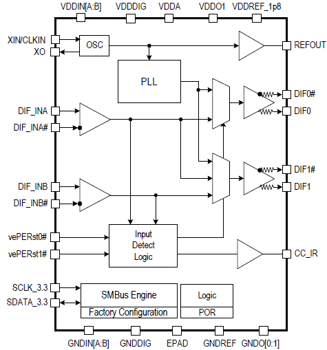
- Automatically detects the presence or absence of input clocks and switches clock modes
- One open-drain CC_IR output indicates PCIe clock mode
- Integrated crystal option available (Q option)
- Two 100MHz Low-power HCSL (LP-HCSL) outputs; 100Ω output impedance
- Integrated terminations on DIF outputs save 8 resistors
- 201, 301 configurations for SRnS (IR) or CC architectures default to 0% SSC
- 202, 302 configurations for SRIS (IR) or CC architectures default to -0.5% SSC
- SMBus-selectable -0.25% SSC
- Choice of 25MHz or 33 1/3MHz reference clock
- REF clock output saves external XO
- 2.5V or 3.3V operating voltage (VDDREF is 1.8V)
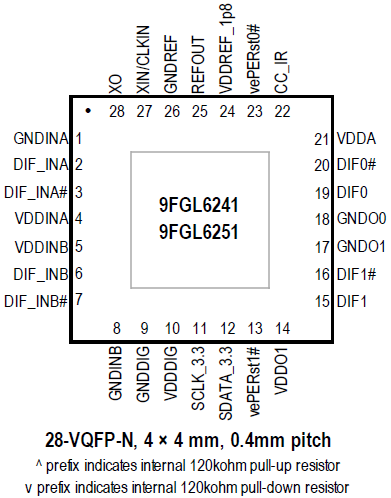
- 4mm × 4mm 28-VQFP-N package with external crystal
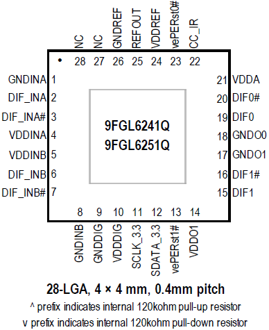
- 4mm × 4mm 28-LGA package with optional internal crystal
- Easy AC coupling to other logic families, see application note AN-891
- For devices with 85Ω output impedance, see 9FGL6251
Description
The 9FGL6241 is an intelligent buffer/clock generator tailored for single and dual-ported nVME SSDs. It supports Common (CC) and Independent Reference (IR) clocking architectures and is ideal for U.2 and M.2 form factors. The device is also useful in PCIe master/slave and clock multiplexing applications, with an internal clock generator as a third input channel.
For information regarding evaluation boards and material, please contact your local sales representative.
Parameters
| Attributes | Value |
|---|---|
| Diff. Outputs | 2 |
| Diff. Output Signaling | LP-HCSL |
| Diff. Inputs | 2 |
| Diff. Input Signaling | HCSL, XTAL, LVCMOS |
| Power Consumption Typ (mW) | 65 |
| Supply Voltage (V) | 3.3 - 3.3 |
| Output Type | LP-HCSL, LVCMOS |
| Xtal Freq (MHz) | 25 - 25, 33.33 - 33.33 |
| Diff. Termination Resistors | 0 |
| Package Area (mm²) | 25 |
| Battery Backup | No |
| Battery Seal | No |
| CPU Supervisory Function POR | No |
| Crystal Frequency Trimming | No |
| Frequency Out Pin | No |
| Inputs (#) | 1 |
| Input Freq (MHz) | 25 - 25, 33.33 - 33.33 |
| Function | Zero Delay Buffer |
| Input Type | Crystal, LVCMOS |
| Output Banks (#) | 1 |
| Product Category | PCI Express Clocks |
Applications
- 1 × 4 and 2 × 2 nVME SSDs
- 3:2 PCIe clock multiplexing