
Features
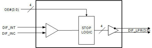
- Four low-power differential output pairs
- Individual OE# control of each output pair
- Output cycle-cycle jitter < 25ps additive
- Output-to-output skew: < 50ps
- Low-power differential fanout buffer for PCI Express and CPU clocks
- Available in commercial (0 °C to +70 °C) and industrial (-40 °C to +85 °C) temperature ranges
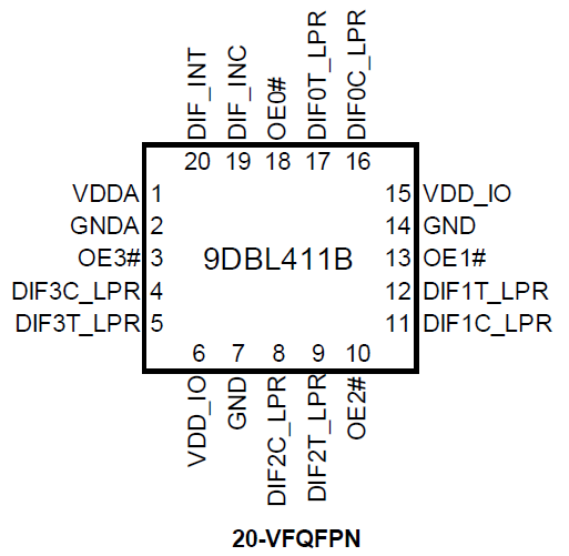
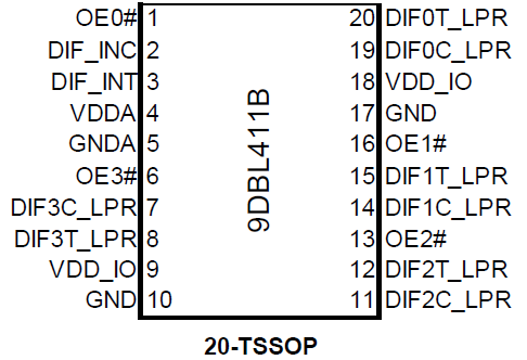
- Available in 20-VFQFPN or 20-TSSOP packages
Description
The 9DBL411 is a four-output lower power differential buffer. Each output has its own OE# pin. The device has a maximum operating frequency of 150MHz.
Parameters
| Attributes | Value |
|---|---|
| Diff. Outputs | 4 |
| Diff. Output Signaling | LP-HCSL |
| Output Freq Range (MHz) | 15 - 150 |
| Diff. Inputs | 1 |
| Diff. Input Signaling | HCSL |
| Accepts Spread Spec Input | Yes |
| Power Consumption Typ (mW) | 132 |
| Supply Voltage (V) | 3.3 - 3.3 |
| Output Type | LP-HCSL |
| Diff. Termination Resistors | 8 |
| Package Area (mm²) | 28.6 |
| Battery Backup | No |
| Battery Seal | No |
| CPU Supervisory Function POR | No |
| Crystal Frequency Trimming | No |
| Frequency Out Pin | No |
| Inputs (#) | 1 |
| Input Freq (MHz) | 15 - 150 |
| Additive Phase Jitter Typ RMS (fs) | 40 |
| Function | Fanout Buffer |
| Input Type | HCSL |
| Output Banks (#) | 1 |
| Core Voltage (V) | 3.3 |
| Output Voltage (V) | 0.8 |
| Product Category | PCI Express Clocks |
Package Options
| Pkg. Type | Pkg. Dimensions (mm) | Lead Count (#) | Pitch (mm) |
|---|---|---|---|
| TSSOP | 6.5 x 4.4 x 1.0 | 20 | 0.65 |