
Features
- One 0.7V current mode differential HCSL output pair
- One differential clock input
- CLK and nCLK supports the following input types: LVPECL, LVDS, LVHSTL, SSTL, HCSL
- Maximum output frequency: 140MHz
- Input frequency range: 90MHz - 140MHz
- VCO range: 450MHz - 700MHz
- Cycle-to-cycle jitter: 30ps (maximum)
- RMS phase jitter @ 100MHz, (1.5MHz - 22MHz): 2.31ps (typical)
- 3.3V operating supply
- 0°C to 70°C ambient operating temperature
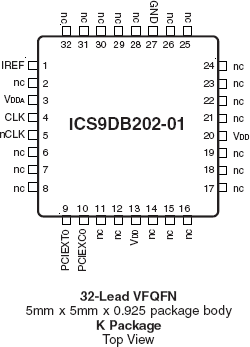
- Available in lead-free RoHS compliant package
- Industrial temperature information available upon request
Description
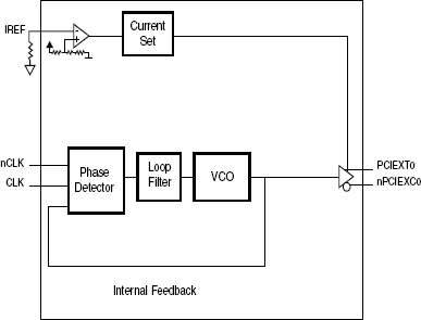
The 9DB202-01 is a high performance 1-to-1 Differential-to HCSL Jitter Attenuator designed for use in PCI Express®™ systems. In some PCI Express® systems, such as those found in desktop PCs, the PCI Express® clocks are generated from a low bandwidth, high phase noise PLL frequency synthesizer. In these systems, a jitter attenuating device may be necessary in order to reduce high frequency random and deterministic jitter components from the PLL synthesizer and from the system board.