
Features
- Six LVCMOS/LVTTL outputs, 20? nominal output impedance
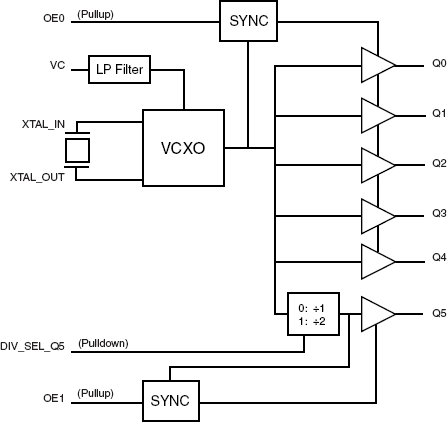
- Output Q5 can be selected for ÷1 or ÷2 frequency relative to the crystal frequency
- Output frequency range: 12MHz to 31.25MHz
- Crystal pull range: ± 90ppm (typical)
- Synchronous output enable places outputs in High-Impedance state
- On-chip filter on VIN to suppress noise modulation of VCXO
- VDD/VDDO combinations 3.3V/3.3V 3.3V/2.5V 3.3V/1.8V 2.5V/2.5V 2.5V/1.8V
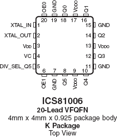
- 4mm x 4mm 20 Lead VFQFN package is ideal for space constrained designs
- 0°C to 70°C ambient operating temperature
- Available in lead-free (RoHS 6) package
Description
The 81006 is a high performance, low jitter/ low phase noise VCXO and is a member of the family of high performance clock solutions from IDT. The 81006 works in conjunction with a pullable crystal to generate an output clock over the range of 12MHz - 31.25MHz and has 6 LVCMOS outputs, effectively integrating a fanout buffer function.
The frequency of the VCXO is adjusted by the VC control voltage input. The output range is ±100ppm around the nominal crystal frequency. The VC control voltage range is 0 - VDD. The device is packaged in a small 4mm x 4mm VFQFN package and is ideal for use on space constrained boards typically encountered in ADSL/VDSL applications.