Features
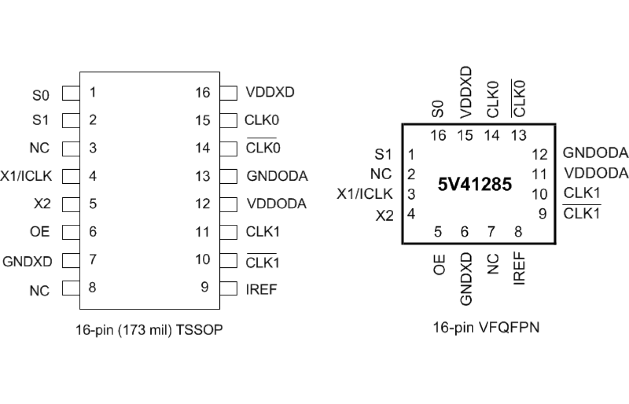
- 16-pin TSSOP and VFQFPN packages; small board footprint
- Outputs can be terminated to LVDS; can drive a wider variety of devices
- OE control pin; greater system power management
- Industrial temperature range available; supports demanding embedded applications
- Cycle-to-cycle jitter: 80ps
- Output-to-output skew <50 ps
- PCIe Gen2 phase jitter <3.0ps RMS
- Low phase noise: 12kHz to 20MHz <6ps
- For PCIe Gen3 applications, see the IDT5V41315
Description
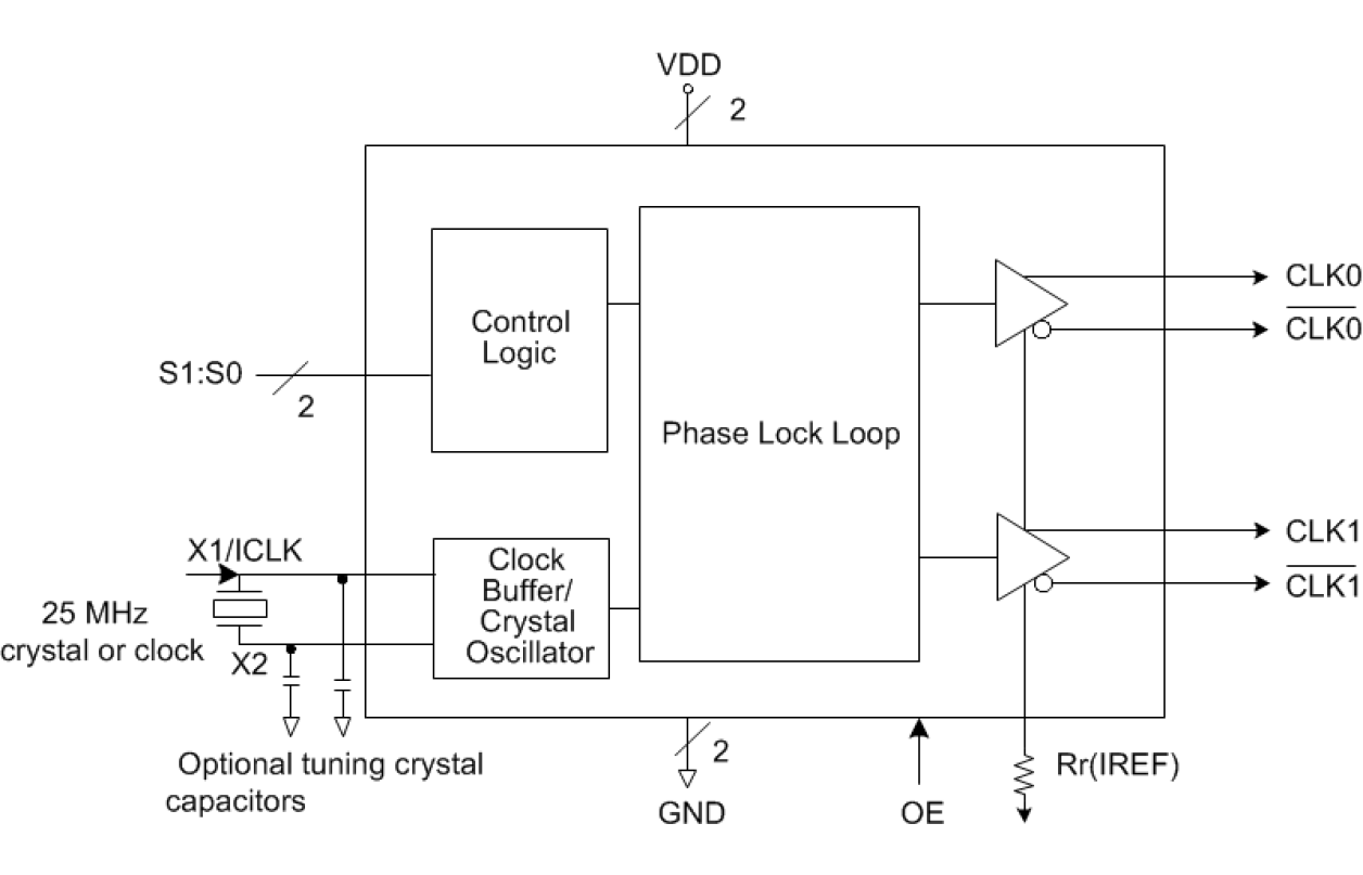
The IDT5V41285 is a PCIe Gen2 compliant clock generator. The device has 2 differential HCSL outputs. The output frequency is selectable via select pins.
Applied Filters:
Filters
Software & Tools
Sample Code
Simulation Models
This is the first video in our PCIe series. In this video, we define PCIe architectures, focusing on common and separate clock architectures. Watch the rest of the video series below where Ron will cover the impact of different timing architectures.
In this episode, Ron Wade from IDT (acquired by Renesas) explains PCIe common clocking and its impact on timing solutions. Learn about using a single clock source, fan-out buffers, and the considerations for spread spectrum and non-spread spectrum clocking in PCIe systems.
In this video, we explore PCIe with separate reference clocks and the effects of clock selection. Learn how separate reference clocks work and their impact on system performance and stability.
This video provides a high-level overview of Separate Reference Clock with Independent Spread (SRIS) architectures for PCI Express systems, additional performance requirements that this clocking architecture imposes on the reference clocks, and some system implications encountered trying to implement the architecture.


