Renesas Electronics Corporation

Renesas’ Timing product portfolio has been acquired by SiTime.

Datasheets, documentation, and sample orders remain available on Renesas.com through late 2026. For new designs, purchasing, support, and product inquiries, visit SiTime.com or send an email to SalesClocks@sitime.com. Full transition to SiTime is expected by late 2026.
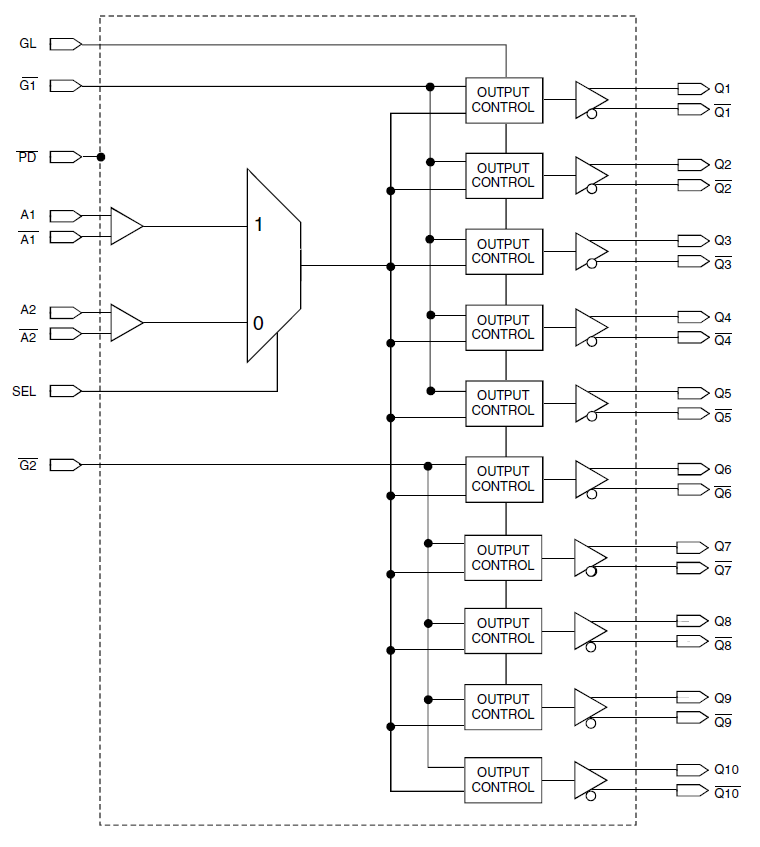
1-to-10 LVDS Fanout Buffer

Package Information

Pkg. Type:VFQFPN
Pkg. Code:NLG40
Lead Count (#):40
Pkg. Dimensions (mm):6.0 x 6.0 x 0.9
Pitch (mm):0.5

Environmental & Export Classifications

Pb (Lead) FreeYes
Moisture Sensitivity Level (MSL)3
ECCN (US)
HTS (US)

Product Attributes

Pkg. TypeVFQFPN
Lead Count (#)40
Pb (Lead) FreeYes
Carrier TypeReel
Core Voltage (V)2.5
FunctionBuffer, Multiplexer
Input Freq (MHz)1000 - 1000
Input TypeLVTTL, HSTL, eHSTL, LVPECL, CML, LVDS
Inputs (#)2
Length (mm)6
MOQ2500
Moisture Sensitivity Level (MSL)3
Output Banks (#)1
Output Freq Range (MHz)1000 - 1000
Output SignalingLVDS
Output Skew (ps)25
Output TypeLVDS
Output Voltage (V)2.5
Outputs (#)10
Package Area (mm²)36
Pb Free Categorye3 Sn
Pitch (mm)0.5
Pkg. Dimensions (mm)6.0 x 6.0 x 0.9
Qty. per Carrier (#)0
Qty. per Reel (#)5000
Reel Size (in)13
Requires Terms and ConditionsDoes not require acceptance of Terms and Conditions
Tape & ReelYes
Temp. Range (°C)-40 to 85°C
Thickness (mm)0.9
Width (mm)6

Description

The 5T9310 is a low skew, 1-to-10 differential LVDS clock fanout buffer. The device has two selectable inputs. The inputs accept LVDS, HSTL, CML, LVPECL and single-ended signals such as 3.3V/2.5V LVCMOS/LVTTL. The 5T9310 outputs can be asynchronously enabled/disabled. When disabled, the outputs will drive to the value selected by the GL pin. Multiple power and grounds reduce noise.