
Features
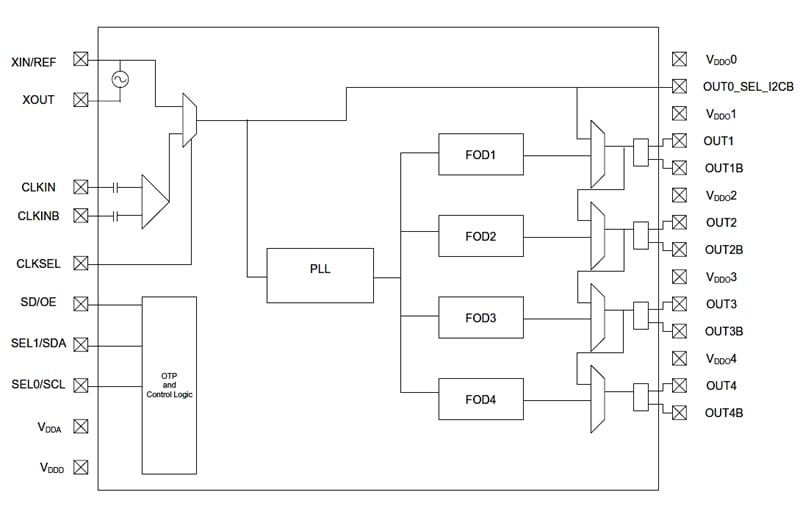
- 4 differential outputs LVPECL, LVDS, HCSL - or 8 LVCMOS outputs
- In-system programmable with 4 independent output frequencies
- Up to 350MHz input/output frequencies
- Also supports crystal input
- Stores 4 different configurations in OTP non-volatile memory
- < 100mW core power (at 3.3V)
- < 0.7ps RMS phase jitter (typ.)
- Meets PCIe® Gen 1/2/3, USB 3.0, 1/10 GbE clock requirements
- 1.8V/2.5V/V3.3V core and output voltages
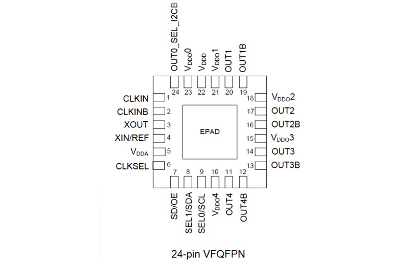
- 4mm x 4mm 24-lead VFQFPN
- -40 °C to +85 °C operating temperature range
- Supported by the Timing Commander™ software tool
Description
The 5P49V5901 is a low-power programmable clock generator with best-in-class jitter performance and design flexibility with universal outputs capable of generating any output frequency. The 5P49V5901 is intended for high-performance consumer, networking, industrial, computing, and data communications applications. Configurations may be stored in on-chip One-Time Programmable (OTP) memory or changed using the I2C interface. This is Renesas' fifth generation of programmable clock technology (VersaClock® 5). The frequencies are generated from a single reference clock or crystal input. A glitchless manual switchover function allows one of the redundant clock inputs to be selected during normal operation.
Two select pins allow up to four different configurations to be programmed and accessible using processor GPIOs or bootstrapping. The different selections may be used for different operating modes (full function, partial function, and partial power-down), regional standards (US, Japan, Europe), or system production margin testing. The device may be configured to use one of two I2C addresses to allow multiple devices to be used in a system.
Parameters
| Attributes | Value |
|---|---|
| App Jitter Compliance | PCIe Gen1, PCIe Gen2, PCIe Gen3 |
| Outputs (#) | 5 |
| Output Type | LVCMOS, LVPECL, HCSL, LVDS |
| Output Freq Range (MHz) | 1 - 350 |
| Input Freq (MHz) | 1 - 350 |
| Inputs (#) | 2 |
| Input Type | Crystal, LVCMOS, LVPECL, LVDS, HCSL |
| Output Banks (#) | 4 |
| Core Voltage (V) | 1.8V, 2.5V, 3.3V |
| Output Voltage (V) | 1.8V, 2.5V, 3.3V |
| Product Category | VersaClock 5, Low Jitter Clocks (<700 fs RMS), General Purpose Clocks, Programmable Clocks |
| Selection Criteria | <700 fs RM |
Package Options
| Pkg. Type | Pkg. Dimensions (mm) | Lead Count (#) | Pitch (mm) |
|---|---|---|---|
| VFQFPN | 4.0 x 4.0 x 0.9 | 24 | 0.5 |
Applications
- Ethernet switches/routers
- PCI Express 1.0/2.0/3.0
- Broadcast video/audio timing
- Multi-function printers
- Processor and FPGA clocking
- Any-frequency clock conversion
- MSAN/DSLAM/PON
- Fiber Channel, SAN
- Telecom line cards
- 1 GbE and 10 GbE
Renesas Boards & Kits
Evaluation Board for 5P49V5901 VersaClock 5
This is the evaluation board for the Renesas 5P49V59xx VersaClock 5 family of programmable clock generators. With RMS phase jitter less than 0.7 picoseconds over the full 12 kHz to 20 MHz integration range, the device meets the stringent jitter requirements of PCI Express® Gen 1/2/3, USB 3.0,... Read More
Support Communities
-
Unable to see output clock from the 5P49V5901 programmable clock generator
... configurations are required? Any suggestions would be greatly appreciated. 全屏 100MHZ_clock_generator_5949V5901.txt 下载 IDT Timing Commander Settings Personality/Version: 5P49V5901 v1.44 Created: 2026-05-15 12:46:54 ------------------------------------------- Part: 5P49V5901 Product Family: VersaClock 5 Company name: mirafra Project Name Ramanujan Operator: Tarun Dash ...
May 15, 2026 -
Reliability >> Failure Rate >> (FIT/MTTF/MTBF) 5P49V5901
Hi, Where could I locate a failure rate (FIT or MTTF or MTFB) for the 5P49V5901 (VersaClock 5 Low Power Programmable Clock Generator)? Thank you, CJR
Jul 24, 2023 -
Trouble in burning OTP for 5P49V5901
Hello I was recently trying to configure the 5P49V5901 chip to desired output frequencies. I am able to do it in the I2C mode which is volatile but I am having trouble burning those configurations onto the chip so that i can make them work on bootup. I am following ...
May 17, 2026

Support Communities


