
Features
- Up to two high-performance universal differential output pairs:
- Low RMS additive phase jitter: 0.2ps
- Four banks of internal non-volatile in-system programmable or factory programmable OTP memory
- I²C serial programming interface
- One additional LVCMOS output clock
- Two universal output pairs:
- Each configurable as one differential output pair or two LVCMOS outputs
- I/O standards:
- Single-ended I/Os: 1.8V to 3.3V LVCMOS
- Differential I/Os: LVPECL, LVDS, and HCSL
- Input frequency ranges:
- LVCMOS reference clock input (XIN/REF) – 1MHz to 200MHz
- LVDS, LVPECL, HCSL differential clock input (CLKIN, CLKINB) – 1MHz to 350MHz
- Crystal frequency range – 8MHz to 40MHz
- Individually selectable output voltage (1.8V, 2.5V, 3.3V) for each output pair
- Redundant clock inputs with manual switchover
- Programmable crystal load capacitance
- Individual output enable/disable
- Power-down mode
- 1.8V, 2.5V or 3.3V core VDDD, VDDA
Description
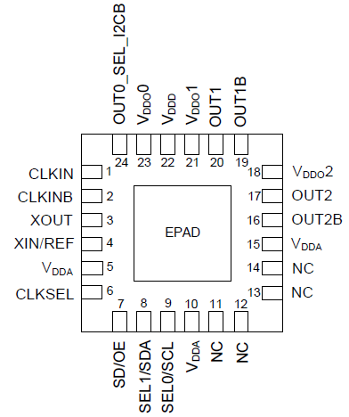
The 5P1103 is a programmable fanout buffer intended for high-performance consumer, networking, industrial, computing, and data communications applications. Configurations may be stored in on-chip One-Time Programmable (OTP) memory or changed using the I²C interface.
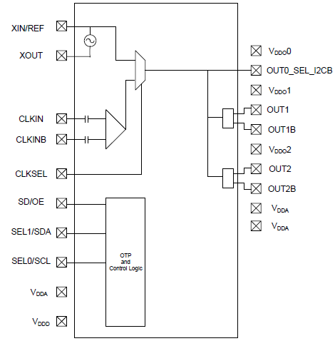
The outputs are generated from a single reference clock. The input reference can be a crystal, external single-ended, or differential clock. The reference clock can come from one of the two redundant clock inputs and is selected by the CLKSEL pin. A glitchless manual switchover function allows one of the redundant clocks to be selected during normal operation. Two select pins allow up to four different configurations to be programmed and accessible using processor GPIOs or bootstrapping. The device is available in a 24-pin VFQFPN 4mm x 4mm package, with an industrial operating temperature range of -40 °C to +85 °C.
Parameters
| Attributes | Value |
|---|---|
| Temp. Range (°C) | -40 to 85°C |
| Product Category | Clock Buffers & Drivers, Clock Multiplexers |
Package Options
| Pkg. Type | Pkg. Dimensions (mm) | Lead Count (#) | Pitch (mm) |
|---|---|---|---|
| VFQFPN | 4.0 x 4.0 x 0.9 | 24 | 0.5 |
Applications
- Ethernet switch/router
- PCI Express 1.0/2.0/3.0
- Broadcast video/audio timing
- Multi-function printer
- Processor and FPGA clocking
- MSAN/DSLAM/PON
- Fiber Channel, SAN
- Telecom line cards
- 1 GbE and 10 GbE
Renesas Boards & Kits
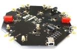
Evaluation Board for 5P1103 Universal Output Buffer
Renesas 5P1103 Programmable buffer outputs can be individually programmed as LVDS, LVPECL, HCSL, or two LVCMOS outputs per output pair, with a crystal, LVCMOS, or differential input. There are up to two universal output pairs, as well as an LVCMOS output clock. Output frequencies range from 1MHz... Read More
Support Communities
-
5P1103 NOT ABLE TO OBTAIN THE OUTPUT CLOCK VOLTAGE
HI, We are using 5P1103A000NLGI in our design. We have connected in I2C Mode and tried to communicate with the chipset. Our input frequency is differential LVPECL : 156.25Mhz. Our requirement : To convert the Differential LVPECL frequency to SIngle ended LVCMOS (3.3V) While probing we are able to attain ...
Apr 24, 2023

Support Communities


