
| CAD Model: | View CAD Model |
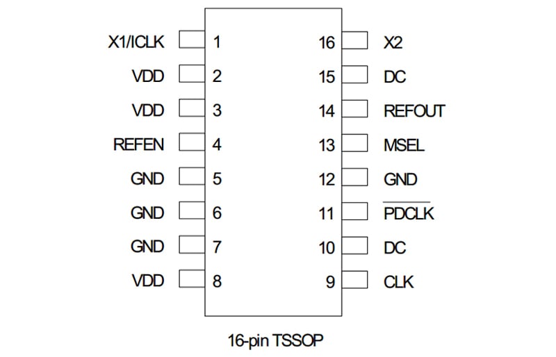
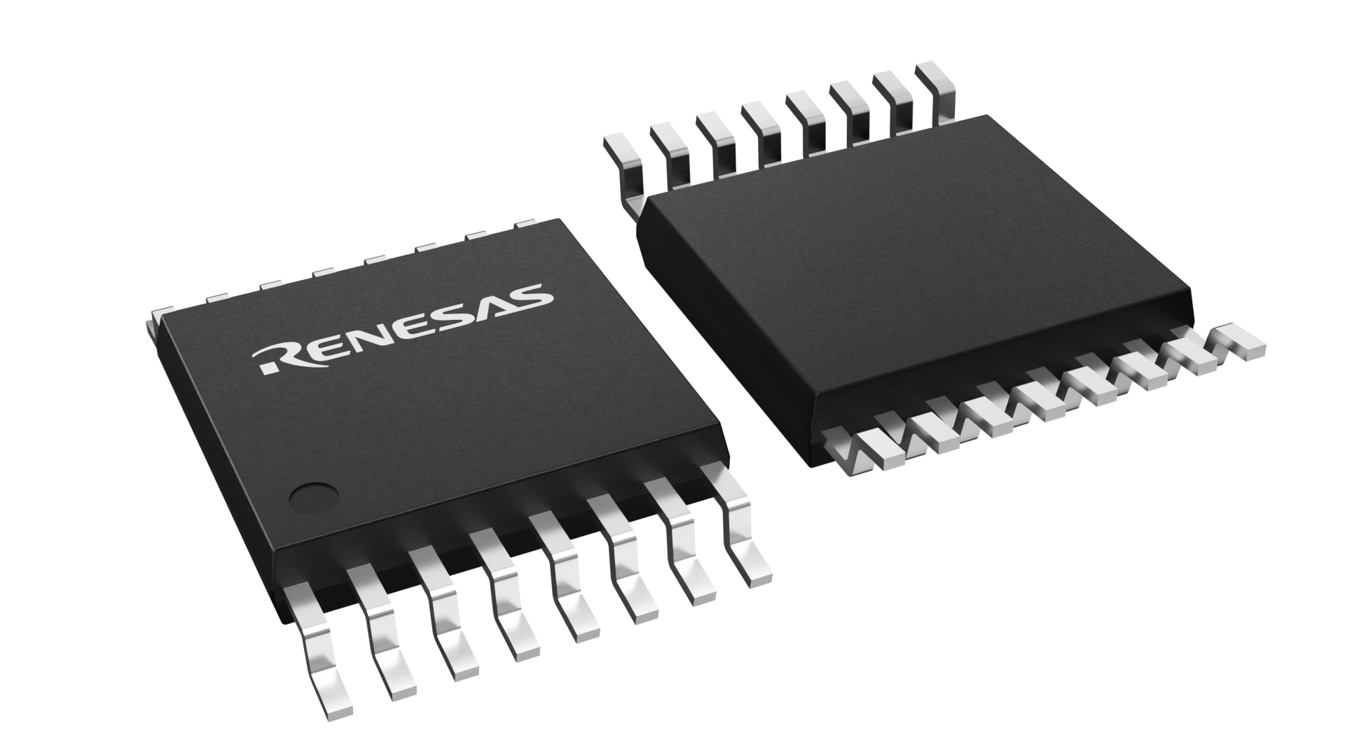
| Pkg. Type: | TSSOP |
| Pkg. Code: | PGG16 |
| Lead Count (#): | 16 |
| Pkg. Dimensions (mm): | 5.0 x 4.4 x 1.0 |
| Pitch (mm): | 0.65 |
| Moisture Sensitivity Level (MSL) | 1 |
| Pb (Lead) Free | Yes |
| ECCN (US) | EAR99 |
| HTS (US) | 8542.39.0090 |
| Lead Count (#) | 16 |
| Carrier Type | Tube |
| Moisture Sensitivity Level (MSL) | 1 |
| Qty. per Reel (#) | 0 |
| Qty. per Carrier (#) | 96 |
| Pb (Lead) Free | Yes |
| Pb Free Category | e3 Sn |
| Temp. Range (°C) | 0 to 70°C |
| Accepts Spread Spec Input | No |
| Advanced Features | Reference Output |
| Clock Spec. | T1, E1 |
| Core Voltage (V) | 3.3V, 5V |
| Feedback Input | No |
| Input Freq (MHz) | 1.544 - 1.544, 2.048 - 2.048 |
| Input Type | Crystal, LVCMOS |
| Inputs (#) | 4 |
| Length (mm) | 5 |
| MOQ | 192 |
| Operating Freq | 24.704, 37.056, 32.768, 49.152 |
| Output Banks (#) | 1 |
| Output Freq Range (MHz) | 24.704 - 24.704, 37.056 - 37.056, 32.768 - 32.768, 49.152 - 49.152 |
| Output Type | LVCMOS |
| Output Voltage (V) | 3.3V, 5V |
| Outputs (#) | 2 |
| Package Area (mm²) | 22 |
| Period Jitter Typ P-P (ps) | 100 |
| Pitch (mm) | 0.65 |
| Pkg. Dimensions (mm) | 5.0 x 4.4 x 1.0 |
| Pkg. Type | TSSOP |
| Product Category | General Purpose Clocks |
| Prog. Clock | No |
| Reference Output | Yes |
| Requires Terms and Conditions | Does not require acceptance of Terms and Conditions |
| Spread Spectrum | No |
| Tape & Reel | No |
| Thickness (mm) | 1 |
| Width (mm) | 4.4 |
| Xtal Freq (KHz) | 1.54 - 1.54 |
| Xtal Inputs (#) | 1 |
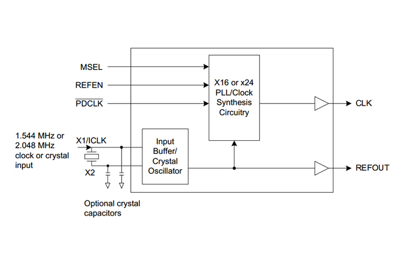
The 548-05 is a low-cost, low-jitter, high-performance clock synthesizer designed to produce x16 and x24 clocks from T1 and E1 frequencies. Using Renesas’ patented analog/digital Phase-Locked Loop (PLL) techniques, the device uses a crystal or clock input to synthesize popular communications frequencies. Power down modes allow the chip to turn off completely, or the PLL and clock output to be turned off separately.
