
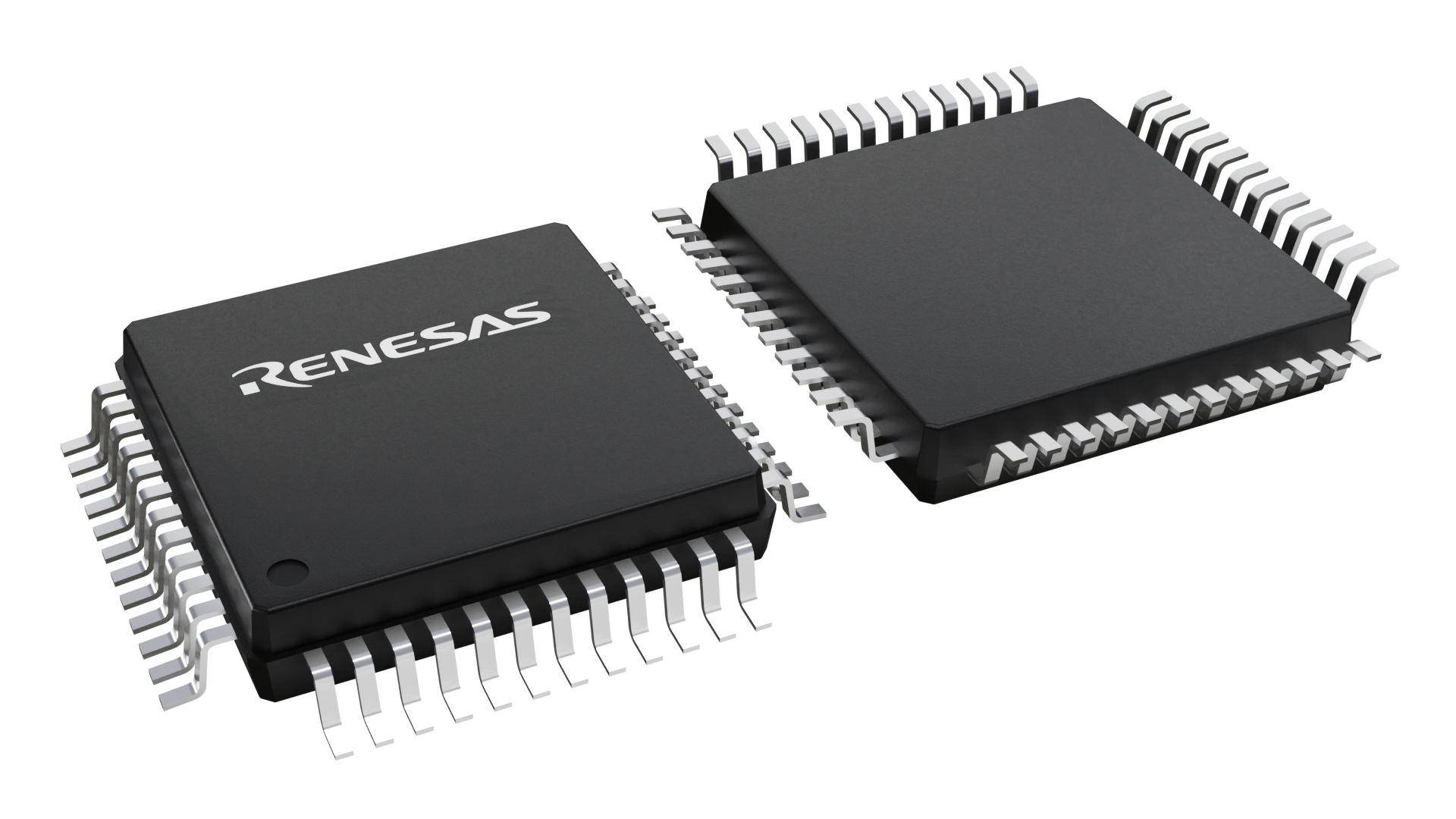

| CAD Model: | View CAD Model |
| Pkg. Type: | TQFP |
| Pkg. Code: | PRG48 |
| Lead Count (#): | 48 |
| Pkg. Dimensions (mm): | 7.0 x 7.0 x 1.4 |
| Pitch (mm): | 0.5 |
| Moisture Sensitivity Level (MSL) | 3 |
| Pb (Lead) Free | Yes |
| ECCN (US) | EAR99 |
| HTS (US) | 8542.39.0090 |
| Lead Count (#) | 48 |
| Carrier Type | Tray |
| Moisture Sensitivity Level (MSL) | 3 |
| Qty. per Reel (#) | 0 |
| Qty. per Carrier (#) | 250 |
| Pb (Lead) Free | Yes |
| Pb Free Category | e3 Sn |
| Temp. Range (°C) | 0 to 70°C |
| Advanced Features | Spread Spectrum |
| C-C Jitter Max P-P (ps) | 35 |
| Core Voltage (V) | 3.3 |
| Divider Value | 2, 4, 5 |
| Feedback Divider | 27 - 33 |
| Feedback Input | No |
| Input Freq (MHz) | 40 |
| Input Type | Crystal, LVCMOS, LVPECL, LVDS, HSTL, HCSL, SSTL |
| Inputs (#) | 4 |
| Length (mm) | 7 |
| MOQ | 250 |
| Output Banks (#) | 4 |
| Output Freq Range (MHz) | 120 - 375 |
| Output Signaling | LVPECL |
| Output Skew (ps) | 120 |
| Output Type | LVPECL |
| Output Voltage (V) | 3.3 |
| Outputs (#) | 4 |
| Package Area (mm²) | 49 |
| Phase Jitter Typ RMS (ps) | 1.33 |
| Pitch (mm) | 0.5 |
| Pkg. Dimensions (mm) | 7.0 x 7.0 x 1.4 |
| Pkg. Type | TQFP |
| Product Category | FemtoClock, Low Jitter Clocks (<700 fs RMS) |
| Prog. Clock | No |
| Reference Output | Yes |
| Requires Terms and Conditions | Does not require acceptance of Terms and Conditions |
| Spread Spectrum | Yes |
| Tape & Reel | No |
| Thickness (mm) | 1.4 |
| VCO Max Freq (MHz) | 640 |
| VCO Min Freq (MHz) | 490 |
| Width (mm) | 7 |
| Xtal Freq (KHz) | 40 |
| Xtal Inputs (#) | 2 |
The 843034-06 is a general purpose, low phase noise LVPECL synthesizer which can generate frequencies for a wide variety of applications. The 843034-06 has a 4:1 input multiplexer from which the following inputs can be selected: one differential input, one single-ended input, or one of two crystal oscillators, thus making the device ideal for frequency translation or frequency generation. The 843034- 06 has dual LVPECL outputs that may be programmed for ÷2, ÷4 or ÷5 of the VCO frequency. The 843034-06 also supplies a buffered copy of the reference clock or crystal frequency on the single-ended REF_OUT pin which can be enabled or disabled (disabled by default). The output frequency can be programmed using either a serial or parallel programming interface. This device supports Spread Spectrum Clocking (SSC) for EMI reduction.