特長
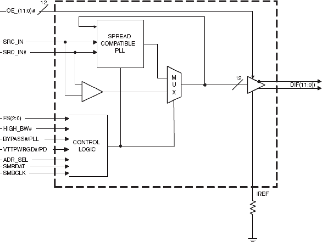
- 12 - 0.7 V current-mode differential output pairs.
- Supports zero delay buffer mode and fanout mode.
- Bandwidth programming available.
- 100-400 MHz operation in PLL mode
- 33-400 MHz operation in Bypass mode
- 3 selectable SMBus addresses for easy system expansion
- Spread spectrum modulation tolerant, 0 to -0.5% down spread and +/- 0.25% center spread
- Supports undriven differential outputs in Power Down Mode for power management.
- Output cycle-cycle jitter < 50 ps
- Output to output skew: 50 ps
- Phase jitter: PCIe Gen2 < 3.1 ps RMS
- Phase jitter: QPI < 0.5 ps RMS
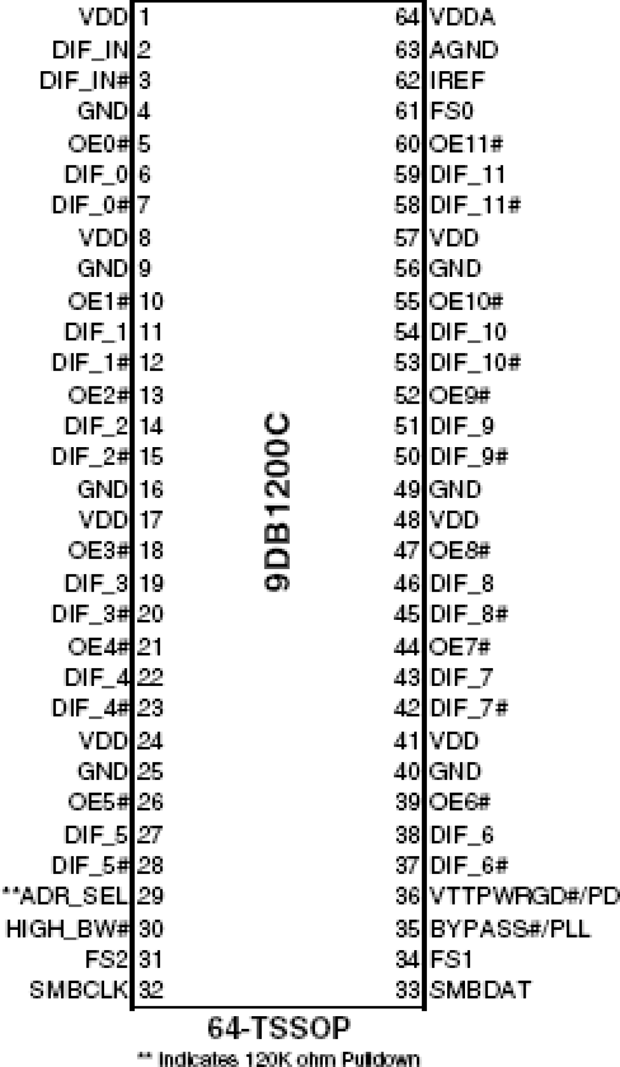
- 64-pin TSSOP Package
- Available in RoHS compliant packaging
説明
The 9DB1200 is an Intel DB1200 Differential Buffer Specification device. This buffer provides 12 differential clocks at frequencies ranging from 100 MHz to 400 MHz. The 9DB1200 is driven by a differential output from a CK410B+ or CK509B main clock generator.
適用されたフィルター


