Customers regularly approach Renesas to solve their entire clock tree. Many times we get requests to solve the entire tree with a single part. That’s OK if there are three to four clocks involved, but we often hear the same thing when there are 20 or more clocks involved. There is a perception that a smaller number of parts with more integrated functions is always better. In the world of analog and mixed-signal, however, this is not always true.
Let’s take a quick look at a few key considerations to take into account when examining the trade-offs between two approaches.
Size/Board Area
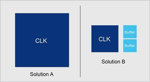
If you need 18 clocks, you have the option of using an 8-output clock in a 40-QFN (6mm x 6mm) plus two 20-QFN (3mm x 3mm) 1 to 6-output buffers. Or, you could simply have a 72-QFN (10mm x 10mm) minimum clock generator.
You can easily see how the difference in the area will affect design size with 54mm2 (Solution B) vs 100mm2 (Solution A) in the figure above.
Flexibility
The fanout buffer solution (B) is much more likely to be re-used in smaller designs, and the buffers can be easily used in multiple scenarios to mix-and-match again.
When there are a lot of clocks required in the system, they are often mixed I/O types (CMOS, LVPECL, HCSL, etc.). Therefore, with a single, large clock generator solution (A), you can either have an extremely flexible large chip or a large chip with lots of re-termination resistors and capacitors. With the fanout solution (B), you have much more flexibility as there are many small, pin-compatible buffers to choose from for these output types.
Signal Integrity
With a single, large packaged part, the layout takes much more effort due to the fact that all of your clock sources are in one place. It’s also harder to make impedance matching on long traces.
Cost
Usually, the costs associated with these larger solutions (A) are very high since bigger clock generators are much more expensive to make. There is an add-on cost when trying to address cross-talk issues and power noise both on-chip and off-chip. Another major concern is the cost associated with re-use. Due to the lack of flexibility of a larger solution (A) when applying this to other projects, the device will be overkill and end up costing more than necessary.
Any Upsides to Solution A?
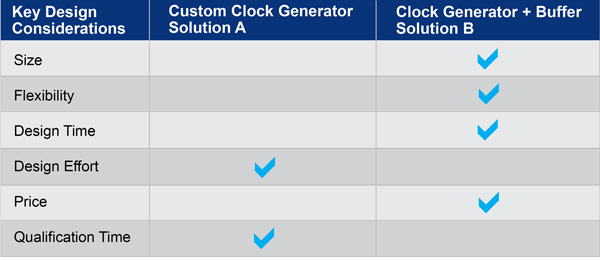
The main advantage of the larger solution is less qualification effort as there are fewer parts. This means less effort in the schematic design, too, but overall this point is debatable since more layout and signal integrity challenges will be introduced.
In general, the systems simply need a clocking solution, not any individual parts in particular. We need to factor in all these considerations when finding a sweet spot between the two options rather than listening to an unconscious bias. I hope this gives you more options for planning your next complex clock tree design.
For more design resources and Buffer selection guides to simplify your clock tree, please visit renesas.com/buffers.
Find details on Renesas' entire industry-leading timing portfolio at renesas.com/timing.