
特長
- Four differential 3.3V LVPECL outputs
- Selectable CLK0 or CLK1 inputs for redundant and multiple frequency fanout applications
- CLK0 or CLK1 can accept the following input levels: LVCMOS or LVTTL
- Maximum output frequency: 266MHz
- Translates LVCMOS and LVTTL levels to 3.3V LVPECL levels
- Output skew: 30ps (maximum)
- Part-to-part skew: 250ps (maximum)
- Propagation delay: 1.9ns (maximum)
- Jitter, RMS: < 0.09ps (typical)
- 3.3V operating supply
- -40°C to 85°C ambient operating temperature
- Available in both standard and lead-free RoHS compliant packages
説明
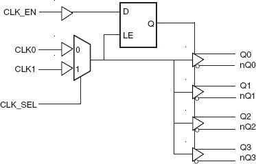
The 8535I-01 is a low skew, high performance 1-to-4 LVCMOS/LVTTL-to-3.3V LVPECL fanout buffer. The 8535I-01 has two single ended clock inputs. the single ended clock input accepts LVCMOS or LVTTL input levels and translate them to 3.3V LVPECL levels. The clock enable is internally synchronized to eliminate runt clock pulses on the output during asynchronous assertion/ deassertion of the clock enable pin. Guaranteed output and part-to-part skew characteristics make the 8535I-01 ideal for those applications demanding well defined performance and repeatability.
パラメータ
| 属性 | 値 |
|---|---|
| Temp. Range (°C) | -40 to 85°C |
| Product Category | Clock Buffers & Drivers, Clock Multiplexers |
パッケージオプション
| Pkg. Type | Pkg. Dimensions (mm) | Lead Count (#) | Pitch (mm) |
|---|---|---|---|
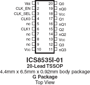
| TSSOP | 6.5 x 4.4 x 1.0 | 20 | 0.65 |