Features
- 32MHz RXv1 core (3.42 CoreMark/MHz*)
- *Typical for RXv1 core
- 1.8V to 3.6V operation, single power supply
- Operating temperature: -40°C to 85°C or -40°C to 105°C
- Built-in Flash memory: 512KB code flash, 64KB SRAM
- 8KB data flash that can store data like an EEPROM
- Diverse package lineup from 36 to 64 pins, including ultra-small 36-pin WFLGA (4.0mm x 4.0mm)
- Up to 46 general-purpose I/O ports
- USB 2.0 Host/Function/OTG (supports full speed (12Mbps), low speed (1.5Mbps), and isochronous transfer)
- Various other communication interfaces (SCI, IIC, RSPI, etc.)
- 16-bit PWM timer, 16-bit compare match timer, RTC
- 12-bit A/D converter, 8-bit D/A converter, temperature sensor


RX111 Block Diagram
Description
The RX111 Group has a comprehensive small-capacity ROM/low pin count lineup. With USB 2.0 for Battery Charging (BC 1.2), low consumption current, and fast wakeup from standby, these microcontrollers are suitable for use in computer peripherals, and healthcare and wearable devices. With their three-phase motor control timers, they are also suitable for motor control applications in home appliances and industrial equipment.
Parameters
| Attributes | Value |
|---|---|
| Main CPU | RXv1 |
| Program Memory (KB) | 16, 32, 64, 96, 128, 256, 384, 512 |
| RAM (KB) | 8, 10, 16, 32, 64 |
| Carrier Type | Bulk (Tray), Full Carton (Tray), Tape & Reel |
| Supply Voltage (V) | 1.8 - 3.6 |
| I/O Ports | 21, 25, 32, 48 |
| DRAM I/F | No |
| Temp. Range (°C) | Ta = -40 to +85, Ta = -40 to +105 |
| Operating Freq (Max) (MHz) | 32 |
| Ethernet speed | No |
| Ethernet (ch) | 0 |
| EtherCat (ch) (#) | 0 |
| USB FS (host ch/device ch) | ( 1 / 1 ) |
| USB HS (host ch/device ch) | ( 0 / 0 ) |
| USB SS (host ch/device ch) | ( 0 / 0 ) |
| SCI or UART (ch) | 3 |
| SPI (ch) | 4 |
| I2C (#) | 4 |
| CAN (ch) | 0 |
| CAN-FD (ch) | 0 |
| Wireless | No |
| SDHI (ch) | 0 |
| High Resolution Output Timer | No |
| PWM Output (pin#) | 12 |
| 32-Bit Timer (ch) | 0 |
| 16-Bit Timer (ch) (#) | 8 |
| 8-Bit Timer (ch) | 0 |
| Standby operable timer | No |
| 12-Bit A/D Converter (ch) | 7, 8, 10, 14 |
| 24-Bit Sigma-Delta A/D Converter (ch) | 0 |
| 16-Bit D/A Converter (ch) | 0 |
| 12-Bit D/A Converter (ch) | 0 |
| 8-Bit D/A Converter (ch) | 0, 2 |
| Capacitive Touch Sensing Unit (ch) | 0 |
| Segment LCD Controller | No |
| Security & Encryption | Unique ID |
Application Block Diagrams
 | Universal NFC Wireless Charger This NFC charger enables the wireless charging of small battery-powered devices ensuring compatibility and user convenience. |
 | AI-Enabled Surveillance Camera AI-powered surveillance camera with DRP-AI boosts security with 4K imaging and low power. |
Additional Applications
- Consumer (battery drive)
- Healthcare
- Home appliances
- Industrial
Complete Your Design
Explore complementary products to elevate your design
RZ/V2M
AI Accelerator (DRP-AI), 4K-compatible Image Signal Processor (ISP), Vision-AI ASSP for Real-time Human and Object Recognition
Datasheet
RAA215300
High-Performance 9-Channel PMIC Supporting DDR Memory, with Built-In Charger and RTC
Datasheet
RAA211630
Integrated FET 60V, 3A Synchronous Buck Regulator with Internal Compensation and Programmable Frequency
Datasheet
RZ/V2N
15TOPS Quad-Core Vision AI MPU with 2-Camera Connection and Excellent Power Efficiency
Datasheet
RA4M2
100MHz Arm Cortex-M33 TrustZone, High Integration With Lowest Active Power Consumption
Datasheet
| Part Number | Status | Samples | Longevity | Stock | Package | Budgetary Price (USD) | Carrier Type | Family Name | Series Name | Group Name | CPU Architecture | Main CPU | Sub CPU | Floating Point Unit | Bit Length | Program Memory (KB) | Data Flash (KB) | RAM (KB) | ECC SRAM | Lead Count (#) | Pitch (mm) | Pkg. Dimensions (mm) | Number of Supply Voltage(s) (#) | Supply Voltage (V) | I/O Ports | DMAC or DTC | DMA (ch) | Temperature Sensor (ch) (#) | Power-On Reset | Watchdog Timer (ch) | External Memory Bus (bit) | DRAM I/F | 3D GPU | Accelerator | MOQ | Temp. Range (°C) | External Interrupt Pins (#) | LVD or PVD | Operating Freq (Max) (MHz) | Sub-clock (32.768 kHz) | On-chip Oscillator | Ethernet speed | Ethernet (ch) | EtherCat (ch) (#) | USB Ports (#) | USB FS (host ch/device ch) | USB HS (host ch/device ch) | USB SS (host ch/device ch) | PCI Express (generation and ch) | SCI or UART (ch) | SPI (ch) | QSPI (ch) | OSPI (ch) | I2C (#) | I3C (ch) | CAN (ch) | CAN-FD (ch) | Wireless | IrDA | LIN (#) | SDHI (ch) | High Resolution Output Timer | PWM Output (pin#) | 32-Bit Timer (ch) | 16-Bit Timer (ch) (#) | 8-Bit Timer (ch) | Standby operable timer | Asynchronous General Purpose Timer / Interval Timer (ch) | RTC | 16-Bit A/D Converter (ch) | 14-Bit A/D Converter (ch) | 12-Bit A/D Converter (ch) | 10-Bit A/D Converter (ch) | 24-Bit Sigma-Delta A/D Converter (ch) | 16-Bit D/A Converter (ch) | 12-Bit D/A Converter (ch) | 10-Bit D/A Converter (ch) (#) | 8-Bit D/A Converter (ch) | Analog Comparator (ch) | OPAMP (ch) (#) | PGA (ch) | Capacitive Touch Sensing Unit (ch) | Graphics LCD Controller | MIPI Interfaces (DSI) (ch) | MIPI Interfaces (CSI) (ch) | Camera I/F (Parallel) | Image Codec | 2D Drawing Engine | Segment LCD Controller | SSI (ch) | Security & Encryption | Debug Interface | Moisture Sensitivity Level (MSL) | Country of Assembly | Country of Wafer Fabrication |
|---|---|---|---|---|---|---|---|---|---|---|---|---|---|---|---|---|---|---|---|---|---|---|---|---|---|---|---|---|---|---|---|---|---|---|---|---|---|---|---|---|---|---|---|---|---|---|---|---|---|---|---|---|---|---|---|---|---|---|---|---|---|---|---|---|---|---|---|---|---|---|---|---|---|---|---|---|---|---|---|---|---|---|---|---|---|---|---|---|---|---|---|---|---|---|---|
| R5F51111ADFK#1A | Active | N/A | 2041 Dec | Out of Stock | LQFP | 1ku | $1.2 | Full Carton (Tray) | RX | RX100 | RX111 | RX | RXv1 | No | No | 32 | 32KB | 8KB | 10KB | No | 64# | 0.8mm | 14 x 14 x 1.7 | 1# | 1.8 - 3.6 | 48 | DTC | 0 | 1# | Yes | 1 | No | No | No | No | 720 | Ta = -40 to +85 | 8# | Yes | 32MHz | Yes | Yes | No | 0 | 0 | 1# | ( 1 / 1 ) | ( 0 / 0 ) | ( 0 / 0 ) | No | 3 | 4 | 0 | 0 | 4# | 0 | 0 | 0 | No | No | 0 | 0 | No | 12 | 0 | 8# | 0 | No | 0 | Yes | 0 | 0 | 14 | 0 | 0 | 0 | 0 | 0 | 2 | 0 | 0 | 0 | 0 | No | 0 | 0 | No | No | No | No | 0 | Unique ID | Single-wire Serial | 3 | CHINA | JAPAN |
| R5F51111ADFK#3A | Active | N/A | In Stock | LQFP | 1ku | $1.2 | Bulk (Tray) | RX | RX100 | RX111 | RX | RXv1 | No | No | 32 | 32KB | 8KB | 10KB | No | 64# | 0.8mm | 14 x 14 x 1.7 | 1# | 1.8 - 3.6 | 48 | DTC | 0 | 1# | Yes | 1 | No | No | No | No | 1 | Ta = -40 to +85 | 8# | Yes | 32MHz | Yes | Yes | No | 0 | 0 | 1# | ( 1 / 1 ) | ( 0 / 0 ) | ( 0 / 0 ) | No | 3 | 4 | 0 | 0 | 4# | 0 | 0 | 0 | No | No | 0 | 0 | No | 12 | 0 | 8# | 0 | No | 0 | Yes | 0 | 0 | 14 | 0 | 0 | 0 | 0 | 0 | 2 | 0 | 0 | 0 | 0 | No | 0 | 0 | No | No | No | No | 0 | Unique ID | Single-wire Serial | 3 | CHINA | JAPAN | |
| R5F51111ADFL#1A | Active | N/A | 2041 Dec | In Stock | LFQFP | 1ku | $1.12 | Full Carton (Tray) | RX | RX100 | RX111 | RX | RXv1 | No | No | 32 | 32KB | 8KB | 10KB | No | 48# | 0.5mm | 7 x 7 x 1.7 | 1# | 1.8 - 3.6 | 32 | DTC | 0 | 1# | Yes | 1 | No | No | No | No | 2000 | Ta = -40 to +85 | 8# | Yes | 32MHz | Yes | Yes | No | 0 | 0 | 1# | ( 1 / 1 ) | ( 0 / 0 ) | ( 0 / 0 ) | No | 3 | 4 | 0 | 0 | 4# | 0 | 0 | 0 | No | No | 0 | 0 | No | 12 | 0 | 8# | 0 | No | 0 | Yes | 0 | 0 | 10 | 0 | 0 | 0 | 0 | 0 | 0 | 0 | 0 | 0 | 0 | No | 0 | 0 | No | No | No | No | 0 | Unique ID | Single-wire Serial | 3 | CHINA | JAPAN |
| R5F51111ADFL#3A | Active | N/A | In Stock | LFQFP | 1ku | $1.12 | Bulk (Tray) | RX | RX100 | RX111 | RX | RXv1 | No | No | 32 | 32KB | 8KB | 10KB | No | 48# | 0.5mm | 7 x 7 x 1.7 | 1# | 1.8 - 3.6 | 32 | DTC | 0 | 1# | Yes | 1 | No | No | No | No | 1 | Ta = -40 to +85 | 8# | Yes | 32MHz | Yes | Yes | No | 0 | 0 | 1# | ( 1 / 1 ) | ( 0 / 0 ) | ( 0 / 0 ) | No | 3 | 4 | 0 | 0 | 4# | 0 | 0 | 0 | No | No | 0 | 0 | No | 12 | 0 | 8# | 0 | No | 0 | Yes | 0 | 0 | 10 | 0 | 0 | 0 | 0 | 0 | 0 | 0 | 0 | 0 | 0 | No | 0 | 0 | No | No | No | No | 0 | Unique ID | Single-wire Serial | 3 | CHINA | JAPAN | |
| R5F51111ADFM#1A | Active | N/A | 2041 Dec | Out of Stock | LFQFP | 1ku | $1.2 | Full Carton (Tray) | RX | RX100 | RX111 | RX | RXv1 | No | No | 32 | 32KB | 8KB | 10KB | No | 64# | 0.5mm | 10 x 10 x 1.7 | 1# | 1.8 - 3.6 | 48 | DTC | 0 | 1# | Yes | 1 | No | No | No | No | 1280 | Ta = -40 to +85 | 8# | Yes | 32MHz | Yes | Yes | No | 0 | 0 | 1# | ( 1 / 1 ) | ( 0 / 0 ) | ( 0 / 0 ) | No | 3 | 4 | 0 | 0 | 4# | 0 | 0 | 0 | No | No | 0 | 0 | No | 12 | 0 | 8# | 0 | No | 0 | Yes | 0 | 0 | 14 | 0 | 0 | 0 | 0 | 0 | 2 | 0 | 0 | 0 | 0 | No | 0 | 0 | No | No | No | No | 0 | Unique ID | Single-wire Serial | 3 | CHINA | JAPAN |
| R5F51111ADFM#3A | Active | N/A | In Stock | LFQFP | 1ku | $1.2 | Bulk (Tray) | RX | RX100 | RX111 | RX | RXv1 | No | No | 32 | 32KB | 8KB | 10KB | No | 64# | 0.5mm | 10 x 10 x 1.7 | 1# | 1.8 - 3.6 | 48 | DTC | 0 | 1# | Yes | 1 | No | No | No | No | 1 | Ta = -40 to +85 | 8# | Yes | 32MHz | Yes | Yes | No | 0 | 0 | 1# | ( 1 / 1 ) | ( 0 / 0 ) | ( 0 / 0 ) | No | 3 | 4 | 0 | 0 | 4# | 0 | 0 | 0 | No | No | 0 | 0 | No | 12 | 0 | 8# | 0 | No | 0 | Yes | 0 | 0 | 14 | 0 | 0 | 0 | 0 | 0 | 2 | 0 | 0 | 0 | 0 | No | 0 | 0 | No | No | No | No | 0 | Unique ID | Single-wire Serial | 3 | CHINA | JAPAN | |
| R5F51111ADNE#0A | Active | N/A | 2036 Dec | Out of Stock | HWQFN | 1ku | $1.12 | Full Carton (Tray) | RX | RX100 | RX111 | RX | RXv1 | No | No | 32 | 32KB | 8KB | 10KB | No | 48# | 0.5mm | 7 x 7 x 0.8 | 1# | 1.8 - 3.6 | 32 | DTC | 0 | 1# | Yes | 1 | No | No | No | No | 3328 | Ta = -40 to +85 | 8# | Yes | 32MHz | Yes | Yes | No | 0 | 0 | 1# | ( 1 / 1 ) | ( 0 / 0 ) | ( 0 / 0 ) | No | 3 | 4 | 0 | 0 | 4# | 0 | 0 | 0 | No | No | 0 | 0 | No | 12 | 0 | 8# | 0 | No | 0 | Yes | 0 | 0 | 10 | 0 | 0 | 0 | 0 | 0 | 0 | 0 | 0 | 0 | 0 | No | 0 | 0 | No | No | No | No | 0 | Unique ID | Single-wire Serial | 3 | TAIWAN | JAPAN |
| R5F51111ADNE#2A | Active | N/A | In Stock | HWQFN | 1ku | $1.12 | Bulk (Tray) | RX | RX100 | RX111 | RX | RXv1 | No | No | 32 | 32KB | 8KB | 10KB | No | 48# | 0.5mm | 7 x 7 x 0.8 | 1# | 1.8 - 3.6 | 32 | DTC | 0 | 1# | Yes | 1 | No | No | No | No | 1 | Ta = -40 to +85 | 8# | Yes | 32MHz | Yes | Yes | No | 0 | 0 | 1# | ( 1 / 1 ) | ( 0 / 0 ) | ( 0 / 0 ) | No | 3 | 4 | 0 | 0 | 4# | 0 | 0 | 0 | No | No | 0 | 0 | No | 12 | 0 | 8# | 0 | No | 0 | Yes | 0 | 0 | 10 | 0 | 0 | 0 | 0 | 0 | 0 | 0 | 0 | 0 | 0 | No | 0 | 0 | No | No | No | No | 0 | Unique ID | Single-wire Serial | 3 | TAIWAN | JAPAN | |
| R5F51111ADNF#0A | Active | N/A | 2036 Dec | Out of Stock | HWQFN | 1ku | $1.06 | Full Carton (Tray) | RX | RX100 | RX111 | RX | RXv1 | No | No | 32 | 32KB | 8KB | 10KB | No | 40# | 0.5mm | 6 x 6 x 0.8 | 1# | 1.8 - 3.6 | 25 | DTC | 0 | 1# | Yes | 1 | No | No | No | No | 3920 | Ta = -40 to +85 | 8# | Yes | 32MHz | No | Yes | No | 0 | 0 | 1# | ( 1 / 1 ) | ( 0 / 0 ) | ( 0 / 0 ) | No | 3 | 4 | 0 | 0 | 4# | 0 | 0 | 0 | No | No | 0 | 0 | No | 12 | 0 | 8# | 0 | No | 0 | No | 0 | 0 | 8 | 0 | 0 | 0 | 0 | 0 | 0 | 0 | 0 | 0 | 0 | No | 0 | 0 | No | No | No | No | 0 | Unique ID | Single-wire Serial | 3 | TAIWAN | JAPAN |
| R5F51111ADNF#2A | Active | N/A | In Stock | HWQFN | 1ku | $1.06 | Bulk (Tray) | RX | RX100 | RX111 | RX | RXv1 | No | No | 32 | 32KB | 8KB | 10KB | No | 40# | 0.5mm | 6 x 6 x 0.8 | 1# | 1.8 - 3.6 | 25 | DTC | 0 | 1# | Yes | 1 | No | No | No | No | 1 | Ta = -40 to +85 | 8# | Yes | 32MHz | No | Yes | No | 0 | 0 | 1# | ( 1 / 1 ) | ( 0 / 0 ) | ( 0 / 0 ) | No | 3 | 4 | 0 | 0 | 4# | 0 | 0 | 0 | No | No | 0 | 0 | No | 12 | 0 | 8# | 0 | No | 0 | No | 0 | 0 | 8 | 0 | 0 | 0 | 0 | 0 | 0 | 0 | 0 | 0 | 0 | No | 0 | 0 | No | No | No | No | 0 | Unique ID | Single-wire Serial | 3 | TAIWAN | JAPAN | |
| R5F51111AGFK#1A | Active | N/A | TBD | Out of Stock | LQFP | 1ku | $1.28 | Full Carton (Tray) | RX | RX100 | RX111 | RX | RXv1 | No | No | 32 | 32KB | 8KB | 10KB | No | 64# | 0.8mm | 14 x 14 x 1.7 | 1# | 1.8 - 3.6 | 48 | DTC | 0 | 1# | Yes | 1 | No | No | No | No | 720 | Ta = -40 to +105 | 8# | Yes | 32MHz | Yes | Yes | No | 0 | 0 | 1# | ( 1 / 1 ) | ( 0 / 0 ) | ( 0 / 0 ) | No | 3 | 4 | 0 | 0 | 4# | 0 | 0 | 0 | No | No | 0 | 0 | No | 12 | 0 | 8# | 0 | No | 0 | Yes | 0 | 0 | 14 | 0 | 0 | 0 | 0 | 0 | 2 | 0 | 0 | 0 | 0 | No | 0 | 0 | No | No | No | No | 0 | Unique ID | Single-wire Serial | 3 | CHINA | JAPAN |
| R5F51111AGFK#3A | Active | N/A | TBD | In Stock | LQFP | 1ku | $1.28 | Bulk (Tray) | RX | RX100 | RX111 | RX | RXv1 | No | No | 32 | 32KB | 8KB | 10KB | No | 64# | 0.8mm | 14 x 14 x 1.7 | 1# | 1.8 - 3.6 | 48 | DTC | 0 | 1# | Yes | 1 | No | No | No | No | 1 | Ta = -40 to +105 | 8# | Yes | 32MHz | Yes | Yes | No | 0 | 0 | 1# | ( 1 / 1 ) | ( 0 / 0 ) | ( 0 / 0 ) | No | 3 | 4 | 0 | 0 | 4# | 0 | 0 | 0 | No | No | 0 | 0 | No | 12 | 0 | 8# | 0 | No | 0 | Yes | 0 | 0 | 14 | 0 | 0 | 0 | 0 | 0 | 2 | 0 | 0 | 0 | 0 | No | 0 | 0 | No | No | No | No | 0 | Unique ID | Single-wire Serial | 3 | CHINA | JAPAN |
| R5F51111AGFL#1A | Active | N/A | TBD | Out of Stock | LFQFP | 1ku | $1.19 | Full Carton (Tray) | RX | RX100 | RX111 | RX | RXv1 | No | No | 32 | 32KB | 8KB | 10KB | No | 48# | 0.5mm | 7 x 7 x 1.7 | 1# | 1.8 - 3.6 | 32 | DTC | 0 | 1# | Yes | 1 | No | No | No | No | 2000 | Ta = -40 to +105 | 8# | Yes | 32MHz | Yes | Yes | No | 0 | 0 | 1# | ( 1 / 1 ) | ( 0 / 0 ) | ( 0 / 0 ) | No | 3 | 4 | 0 | 0 | 4# | 0 | 0 | 0 | No | No | 0 | 0 | No | 12 | 0 | 8# | 0 | No | 0 | Yes | 0 | 0 | 10 | 0 | 0 | 0 | 0 | 0 | 0 | 0 | 0 | 0 | 0 | No | 0 | 0 | No | No | No | No | 0 | Unique ID | Single-wire Serial | 3 | CHINA | JAPAN |
| R5F51111AGFL#3A | Active | N/A | TBD | In Stock | LFQFP | 1ku | $1.19 | Bulk (Tray) | RX | RX100 | RX111 | RX | RXv1 | No | No | 32 | 32KB | 8KB | 10KB | No | 48# | 0.5mm | 7 x 7 x 1.7 | 1# | 1.8 - 3.6 | 32 | DTC | 0 | 1# | Yes | 1 | No | No | No | No | 1 | Ta = -40 to +105 | 8# | Yes | 32MHz | Yes | Yes | No | 0 | 0 | 1# | ( 1 / 1 ) | ( 0 / 0 ) | ( 0 / 0 ) | No | 3 | 4 | 0 | 0 | 4# | 0 | 0 | 0 | No | No | 0 | 0 | No | 12 | 0 | 8# | 0 | No | 0 | Yes | 0 | 0 | 10 | 0 | 0 | 0 | 0 | 0 | 0 | 0 | 0 | 0 | 0 | No | 0 | 0 | No | No | No | No | 0 | Unique ID | Single-wire Serial | 3 | CHINA | JAPAN |
| R5F51111AGFM#1A | Active | N/A | TBD | Out of Stock | LFQFP | 1ku | $1.28 | Full Carton (Tray) | RX | RX100 | RX111 | RX | RXv1 | No | No | 32 | 32KB | 8KB | 10KB | No | 64# | 0.5mm | 10 x 10 x 1.7 | 1# | 1.8 - 3.6 | 48 | DTC | 0 | 1# | Yes | 1 | No | No | No | No | 1280 | Ta = -40 to +105 | 8# | Yes | 32MHz | Yes | Yes | No | 0 | 0 | 1# | ( 1 / 1 ) | ( 0 / 0 ) | ( 0 / 0 ) | No | 3 | 4 | 0 | 0 | 4# | 0 | 0 | 0 | No | No | 0 | 0 | No | 12 | 0 | 8# | 0 | No | 0 | Yes | 0 | 0 | 14 | 0 | 0 | 0 | 0 | 0 | 2 | 0 | 0 | 0 | 0 | No | 0 | 0 | No | No | No | No | 0 | Unique ID | Single-wire Serial | 3 | CHINA | JAPAN |
| R5F51111AGFM#3A | Active | N/A | TBD | In Stock | LFQFP | 1ku | $1.28 | Bulk (Tray) | RX | RX100 | RX111 | RX | RXv1 | No | No | 32 | 32KB | 8KB | 10KB | No | 64# | 0.5mm | 10 x 10 x 1.7 | 1# | 1.8 - 3.6 | 48 | DTC | 0 | 1# | Yes | 1 | No | No | No | No | 1 | Ta = -40 to +105 | 8# | Yes | 32MHz | Yes | Yes | No | 0 | 0 | 1# | ( 1 / 1 ) | ( 0 / 0 ) | ( 0 / 0 ) | No | 3 | 4 | 0 | 0 | 4# | 0 | 0 | 0 | No | No | 0 | 0 | No | 12 | 0 | 8# | 0 | No | 0 | Yes | 0 | 0 | 14 | 0 | 0 | 0 | 0 | 0 | 2 | 0 | 0 | 0 | 0 | No | 0 | 0 | No | No | No | No | 0 | Unique ID | Single-wire Serial | 3 | CHINA | JAPAN |
| R5F51111AGNE#0A | Active | N/A | Out of Stock | HWQFN | 1ku | $1.19 | Full Carton (Tray) | RX | RX100 | RX111 | RX | RXv1 | No | No | 32 | 32KB | 8KB | 10KB | No | 48# | 0.5mm | 7 x 7 x 0.8 | 1# | 1.8 - 3.6 | 32 | DTC | 0 | 1# | Yes | 1 | No | No | No | No | 3328 | Ta = -40 to +105 | 8# | Yes | 32MHz | Yes | Yes | No | 0 | 0 | 1# | ( 1 / 1 ) | ( 0 / 0 ) | ( 0 / 0 ) | No | 3 | 4 | 0 | 0 | 4# | 0 | 0 | 0 | No | No | 0 | 0 | No | 12 | 0 | 8# | 0 | No | 0 | Yes | 0 | 0 | 10 | 0 | 0 | 0 | 0 | 0 | 0 | 0 | 0 | 0 | 0 | No | 0 | 0 | No | No | No | No | 0 | Unique ID | Single-wire Serial | 3 | TAIWAN | JAPAN | |
| R5F51111AGNE#2A | Active | N/A | In Stock | HWQFN | 1ku | $1.19 | Bulk (Tray) | RX | RX100 | RX111 | RX | RXv1 | No | No | 32 | 32KB | 8KB | 10KB | No | 48# | 0.5mm | 7 x 7 x 0.8 | 1# | 1.8 - 3.6 | 32 | DTC | 0 | 1# | Yes | 1 | No | No | No | No | 1 | Ta = -40 to +105 | 8# | Yes | 32MHz | Yes | Yes | No | 0 | 0 | 1# | ( 1 / 1 ) | ( 0 / 0 ) | ( 0 / 0 ) | No | 3 | 4 | 0 | 0 | 4# | 0 | 0 | 0 | No | No | 0 | 0 | No | 12 | 0 | 8# | 0 | No | 0 | Yes | 0 | 0 | 10 | 0 | 0 | 0 | 0 | 0 | 0 | 0 | 0 | 0 | 0 | No | 0 | 0 | No | No | No | No | 0 | Unique ID | Single-wire Serial | 3 | TAIWAN | JAPAN | |
| R5F51111AGNF#0A | Active | N/A | 2036 Dec | Out of Stock | HWQFN | 1ku | $1.14 | Full Carton (Tray) | RX | RX100 | RX111 | RX | RXv1 | No | No | 32 | 32KB | 8KB | 10KB | No | 40# | 0.5mm | 6 x 6 x 0.8 | 1# | 1.8 - 3.6 | 25 | DTC | 0 | 1# | Yes | 1 | No | No | No | No | 3920 | Ta = -40 to +105 | 8# | Yes | 32MHz | No | Yes | No | 0 | 0 | 1# | ( 1 / 1 ) | ( 0 / 0 ) | ( 0 / 0 ) | No | 3 | 4 | 0 | 0 | 4# | 0 | 0 | 0 | No | No | 0 | 0 | No | 12 | 0 | 8# | 0 | No | 0 | No | 0 | 0 | 8 | 0 | 0 | 0 | 0 | 0 | 0 | 0 | 0 | 0 | 0 | No | 0 | 0 | No | No | No | No | 0 | Unique ID | Single-wire Serial | 3 | TAIWAN | JAPAN |
| R5F51111AGNF#2A | Active | N/A | In Stock | HWQFN | 1ku | $1.14 | Bulk (Tray) | RX | RX100 | RX111 | RX | RXv1 | No | No | 32 | 32KB | 8KB | 10KB | No | 40# | 0.5mm | 6 x 6 x 0.8 | 1# | 1.8 - 3.6 | 25 | DTC | 0 | 1# | Yes | 1 | No | No | No | No | 1 | Ta = -40 to +105 | 8# | Yes | 32MHz | No | Yes | No | 0 | 0 | 1# | ( 1 / 1 ) | ( 0 / 0 ) | ( 0 / 0 ) | No | 3 | 4 | 0 | 0 | 4# | 0 | 0 | 0 | No | No | 0 | 0 | No | 12 | 0 | 8# | 0 | No | 0 | No | 0 | 0 | 8 | 0 | 0 | 0 | 0 | 0 | 0 | 0 | 0 | 0 | 0 | No | 0 | 0 | No | No | No | No | 0 | Unique ID | Single-wire Serial | 3 | TAIWAN | JAPAN | |
| R5F51113ADFK#1A | Active | N/A | 2041 Dec | Out of Stock | LQFP | 1ku | $1.26 | Full Carton (Tray) | RX | RX100 | RX111 | RX | RXv1 | No | No | 32 | 64KB | 8KB | 10KB | No | 64# | 0.8mm | 14 x 14 x 1.7 | 1# | 1.8 - 3.6 | 48 | DTC | 0 | 1# | Yes | 1 | No | No | No | No | 720 | Ta = -40 to +85 | 8# | Yes | 32MHz | Yes | Yes | No | 0 | 0 | 1# | ( 1 / 1 ) | ( 0 / 0 ) | ( 0 / 0 ) | No | 3 | 4 | 0 | 0 | 4# | 0 | 0 | 0 | No | No | 0 | 0 | No | 12 | 0 | 8# | 0 | No | 0 | Yes | 0 | 0 | 14 | 0 | 0 | 0 | 0 | 0 | 2 | 0 | 0 | 0 | 0 | No | 0 | 0 | No | No | No | No | 0 | Unique ID | Single-wire Serial | 3 | CHINA | JAPAN |
| R5F51113ADFK#3A | Active | N/A | In Stock | LQFP | 1ku | $1.26 | Bulk (Tray) | RX | RX100 | RX111 | RX | RXv1 | No | No | 32 | 64KB | 8KB | 10KB | No | 64# | 0.8mm | 14 x 14 x 1.7 | 1# | 1.8 - 3.6 | 48 | DTC | 0 | 1# | Yes | 1 | No | No | No | No | 1 | Ta = -40 to +85 | 8# | Yes | 32MHz | Yes | Yes | No | 0 | 0 | 1# | ( 1 / 1 ) | ( 0 / 0 ) | ( 0 / 0 ) | No | 3 | 4 | 0 | 0 | 4# | 0 | 0 | 0 | No | No | 0 | 0 | No | 12 | 0 | 8# | 0 | No | 0 | Yes | 0 | 0 | 14 | 0 | 0 | 0 | 0 | 0 | 2 | 0 | 0 | 0 | 0 | No | 0 | 0 | No | No | No | No | 0 | Unique ID | Single-wire Serial | 3 | CHINA | JAPAN | |
| R5F51113ADFL#1A | Active | N/A | 2041 Dec | Out of Stock | LFQFP | 1ku | $1.17 | Full Carton (Tray) | RX | RX100 | RX111 | RX | RXv1 | No | No | 32 | 64KB | 8KB | 10KB | No | 48# | 0.5mm | 7 x 7 x 1.7 | 1# | 1.8 - 3.6 | 32 | DTC | 0 | 1# | Yes | 1 | No | No | No | No | 2000 | Ta = -40 to +85 | 8# | Yes | 32MHz | Yes | Yes | No | 0 | 0 | 1# | ( 1 / 1 ) | ( 0 / 0 ) | ( 0 / 0 ) | No | 3 | 4 | 0 | 0 | 4# | 0 | 0 | 0 | No | No | 0 | 0 | No | 12 | 0 | 8# | 0 | No | 0 | Yes | 0 | 0 | 10 | 0 | 0 | 0 | 0 | 0 | 0 | 0 | 0 | 0 | 0 | No | 0 | 0 | No | No | No | No | 0 | Unique ID | Single-wire Serial | 3 | CHINA | JAPAN |
| R5F51113ADFL#3A | Active | N/A | In Stock | LFQFP | 1ku | $1.17 | Bulk (Tray) | RX | RX100 | RX111 | RX | RXv1 | No | No | 32 | 64KB | 8KB | 10KB | No | 48# | 0.5mm | 7 x 7 x 1.7 | 1# | 1.8 - 3.6 | 32 | DTC | 0 | 1# | Yes | 1 | No | No | No | No | 1 | Ta = -40 to +85 | 8# | Yes | 32MHz | Yes | Yes | No | 0 | 0 | 1# | ( 1 / 1 ) | ( 0 / 0 ) | ( 0 / 0 ) | No | 3 | 4 | 0 | 0 | 4# | 0 | 0 | 0 | No | No | 0 | 0 | No | 12 | 0 | 8# | 0 | No | 0 | Yes | 0 | 0 | 10 | 0 | 0 | 0 | 0 | 0 | 0 | 0 | 0 | 0 | 0 | No | 0 | 0 | No | No | No | No | 0 | Unique ID | Single-wire Serial | 3 | CHINA | JAPAN | |
| R5F51113ADFM#1A | Active | N/A | 2041 Dec | In Stock | LFQFP | 1ku | $1.26 | Full Carton (Tray) | RX | RX100 | RX111 | RX | RXv1 | No | No | 32 | 64KB | 8KB | 10KB | No | 64# | 0.5mm | 10 x 10 x 1.7 | 1# | 1.8 - 3.6 | 48 | DTC | 0 | 1# | Yes | 1 | No | No | No | No | 1280 | Ta = -40 to +85 | 8# | Yes | 32MHz | Yes | Yes | No | 0 | 0 | 1# | ( 1 / 1 ) | ( 0 / 0 ) | ( 0 / 0 ) | No | 3 | 4 | 0 | 0 | 4# | 0 | 0 | 0 | No | No | 0 | 0 | No | 12 | 0 | 8# | 0 | No | 0 | Yes | 0 | 0 | 14 | 0 | 0 | 0 | 0 | 0 | 2 | 0 | 0 | 0 | 0 | No | 0 | 0 | No | No | No | No | 0 | Unique ID | Single-wire Serial | 3 | CHINA | JAPAN |
| R5F51113ADFM#3A | Active | N/A | In Stock | LFQFP | 1ku | $1.26 | Bulk (Tray) | RX | RX100 | RX111 | RX | RXv1 | No | No | 32 | 64KB | 8KB | 10KB | No | 64# | 0.5mm | 10 x 10 x 1.7 | 1# | 1.8 - 3.6 | 48 | DTC | 0 | 1# | Yes | 1 | No | No | No | No | 1 | Ta = -40 to +85 | 8# | Yes | 32MHz | Yes | Yes | No | 0 | 0 | 1# | ( 1 / 1 ) | ( 0 / 0 ) | ( 0 / 0 ) | No | 3 | 4 | 0 | 0 | 4# | 0 | 0 | 0 | No | No | 0 | 0 | No | 12 | 0 | 8# | 0 | No | 0 | Yes | 0 | 0 | 14 | 0 | 0 | 0 | 0 | 0 | 2 | 0 | 0 | 0 | 0 | No | 0 | 0 | No | No | No | No | 0 | Unique ID | Single-wire Serial | 3 | CHINA | JAPAN | |
| R5F51113ADLM#GA | Active | N/A | Out of Stock | WFLGA | 1ku | $1.13 | Full Carton (Tray) | RX | RX100 | RX111 | RX | RXv1 | No | No | 32 | 64KB | 8KB | 10KB | No | 36# | 0.5mm | 4 x 4 x 0.76 | 1# | 1.8 - 3.6 | 21 | DTC | 0 | 1# | Yes | 1 | No | No | No | No | 3920 | Ta = -40 to +85 | 8# | Yes | 32MHz | No | Yes | No | 0 | 0 | 1# | ( 1 / 1 ) | ( 0 / 0 ) | ( 0 / 0 ) | No | 3 | 4 | 0 | 0 | 4# | 0 | 0 | 0 | No | No | 0 | 0 | No | 12 | 0 | 8# | 0 | No | 0 | No | 0 | 0 | 7 | 0 | 0 | 0 | 0 | 0 | 0 | 0 | 0 | 0 | 0 | No | 0 | 0 | No | No | No | No | 0 | Unique ID | Single-wire Serial | 3 | MALAYSIA | JAPAN | |
| R5F51113ADLM#UA | Active | Available | TBD | In Stock | WFLGA | 1ku | $1.13 | Bulk (Tray) | RX | RX100 | RX111 | RX | RXv1 | No | No | 32 | 64KB | 8KB | 10KB | No | 36# | 0.5mm | 4 x 4 x 0.76 | 1# | 1.8 - 3.6 | 21 | DTC | 0 | 1# | Yes | 1 | No | No | No | No | 1 | Ta = -40 to +85 | 8# | Yes | 32MHz | No | Yes | No | 0 | 0 | 1# | ( 1 / 1 ) | ( 0 / 0 ) | ( 0 / 0 ) | No | 3 | 4 | 0 | 0 | 4# | 0 | 0 | 0 | No | No | 0 | 0 | No | 12 | 0 | 8# | 0 | No | 0 | No | 0 | 0 | 7 | 0 | 0 | 0 | 0 | 0 | 0 | 0 | 0 | 0 | 0 | No | 0 | 0 | No | No | No | No | 0 | Unique ID | Single-wire Serial | 3 | MALAYSIA | JAPAN |
| R5F51113ADNE#0A | Active | N/A | 2036 Dec | Out of Stock | HWQFN | 1ku | $1.17 | Full Carton (Tray) | RX | RX100 | RX111 | RX | RXv1 | No | No | 32 | 64KB | 8KB | 10KB | No | 48# | 0.5mm | 7 x 7 x 0.8 | 1# | 1.8 - 3.6 | 32 | DTC | 0 | 1# | Yes | 1 | No | No | No | No | 3328 | Ta = -40 to +85 | 8# | Yes | 32MHz | Yes | Yes | No | 0 | 0 | 1# | ( 1 / 1 ) | ( 0 / 0 ) | ( 0 / 0 ) | No | 3 | 4 | 0 | 0 | 4# | 0 | 0 | 0 | No | No | 0 | 0 | No | 12 | 0 | 8# | 0 | No | 0 | Yes | 0 | 0 | 10 | 0 | 0 | 0 | 0 | 0 | 0 | 0 | 0 | 0 | 0 | No | 0 | 0 | No | No | No | No | 0 | Unique ID | Single-wire Serial | 3 | TAIWAN | JAPAN |
| R5F51113ADNE#2A | Active | N/A | In Stock | HWQFN | 1ku | $1.17 | Bulk (Tray) | RX | RX100 | RX111 | RX | RXv1 | No | No | 32 | 64KB | 8KB | 10KB | No | 48# | 0.5mm | 7 x 7 x 0.8 | 1# | 1.8 - 3.6 | 32 | DTC | 0 | 1# | Yes | 1 | No | No | No | No | 1 | Ta = -40 to +85 | 8# | Yes | 32MHz | Yes | Yes | No | 0 | 0 | 1# | ( 1 / 1 ) | ( 0 / 0 ) | ( 0 / 0 ) | No | 3 | 4 | 0 | 0 | 4# | 0 | 0 | 0 | No | No | 0 | 0 | No | 12 | 0 | 8# | 0 | No | 0 | Yes | 0 | 0 | 10 | 0 | 0 | 0 | 0 | 0 | 0 | 0 | 0 | 0 | 0 | No | 0 | 0 | No | No | No | No | 0 | Unique ID | Single-wire Serial | 3 | TAIWAN | JAPAN | |
| R5F51113ADNF#0A | Active | N/A | 2036 Dec | Out of Stock | HWQFN | 1ku | $1.13 | Full Carton (Tray) | RX | RX100 | RX111 | RX | RXv1 | No | No | 32 | 64KB | 8KB | 10KB | No | 40# | 0.5mm | 6 x 6 x 0.8 | 1# | 1.8 - 3.6 | 25 | DTC | 0 | 1# | Yes | 1 | No | No | No | No | 3920 | Ta = -40 to +85 | 8# | Yes | 32MHz | No | Yes | No | 0 | 0 | 1# | ( 1 / 1 ) | ( 0 / 0 ) | ( 0 / 0 ) | No | 3 | 4 | 0 | 0 | 4# | 0 | 0 | 0 | No | No | 0 | 0 | No | 12 | 0 | 8# | 0 | No | 0 | No | 0 | 0 | 8 | 0 | 0 | 0 | 0 | 0 | 0 | 0 | 0 | 0 | 0 | No | 0 | 0 | No | No | No | No | 0 | Unique ID | Single-wire Serial | 3 | TAIWAN | JAPAN |
| R5F51113ADNF#2A | Active | N/A | In Stock | HWQFN | 1ku | $1.13 | Bulk (Tray) | RX | RX100 | RX111 | RX | RXv1 | No | No | 32 | 64KB | 8KB | 10KB | No | 40# | 0.5mm | 6 x 6 x 0.8 | 1# | 1.8 - 3.6 | 25 | DTC | 0 | 1# | Yes | 1 | No | No | No | No | 1 | Ta = -40 to +85 | 8# | Yes | 32MHz | No | Yes | No | 0 | 0 | 1# | ( 1 / 1 ) | ( 0 / 0 ) | ( 0 / 0 ) | No | 3 | 4 | 0 | 0 | 4# | 0 | 0 | 0 | No | No | 0 | 0 | No | 12 | 0 | 8# | 0 | No | 0 | No | 0 | 0 | 8 | 0 | 0 | 0 | 0 | 0 | 0 | 0 | 0 | 0 | 0 | No | 0 | 0 | No | No | No | No | 0 | Unique ID | Single-wire Serial | 3 | TAIWAN | JAPAN | |
| R5F51113AGFK#1A | Active | N/A | TBD | Out of Stock | LQFP | 1ku | $1.36 | Full Carton (Tray) | RX | RX100 | RX111 | RX | RXv1 | No | No | 32 | 64KB | 8KB | 10KB | No | 64# | 0.8mm | 14 x 14 x 1.7 | 1# | 1.8 - 3.6 | 48 | DTC | 0 | 1# | Yes | 1 | No | No | No | No | 720 | Ta = -40 to +105 | 8# | Yes | 32MHz | Yes | Yes | No | 0 | 0 | 1# | ( 1 / 1 ) | ( 0 / 0 ) | ( 0 / 0 ) | No | 3 | 4 | 0 | 0 | 4# | 0 | 0 | 0 | No | No | 0 | 0 | No | 12 | 0 | 8# | 0 | No | 0 | Yes | 0 | 0 | 14 | 0 | 0 | 0 | 0 | 0 | 2 | 0 | 0 | 0 | 0 | No | 0 | 0 | No | No | No | No | 0 | Unique ID | Single-wire Serial | 3 | CHINA | JAPAN |
| R5F51113AGFK#3A | Active | N/A | TBD | In Stock | LQFP | 1ku | $1.36 | Bulk (Tray) | RX | RX100 | RX111 | RX | RXv1 | No | No | 32 | 64KB | 8KB | 10KB | No | 64# | 0.8mm | 14 x 14 x 1.7 | 1# | 1.8 - 3.6 | 48 | DTC | 0 | 1# | Yes | 1 | No | No | No | No | 1 | Ta = -40 to +105 | 8# | Yes | 32MHz | Yes | Yes | No | 0 | 0 | 1# | ( 1 / 1 ) | ( 0 / 0 ) | ( 0 / 0 ) | No | 3 | 4 | 0 | 0 | 4# | 0 | 0 | 0 | No | No | 0 | 0 | No | 12 | 0 | 8# | 0 | No | 0 | Yes | 0 | 0 | 14 | 0 | 0 | 0 | 0 | 0 | 2 | 0 | 0 | 0 | 0 | No | 0 | 0 | No | No | No | No | 0 | Unique ID | Single-wire Serial | 3 | CHINA | JAPAN |
| R5F51113AGFL#1A | Active | N/A | TBD | In Stock | LFQFP | 1ku | $1.25 | Full Carton (Tray) | RX | RX100 | RX111 | RX | RXv1 | No | No | 32 | 64KB | 8KB | 10KB | No | 48# | 0.5mm | 7 x 7 x 1.7 | 1# | 1.8 - 3.6 | 32 | DTC | 0 | 1# | Yes | 1 | No | No | No | No | 2000 | Ta = -40 to +105 | 8# | Yes | 32MHz | Yes | Yes | No | 0 | 0 | 1# | ( 1 / 1 ) | ( 0 / 0 ) | ( 0 / 0 ) | No | 3 | 4 | 0 | 0 | 4# | 0 | 0 | 0 | No | No | 0 | 0 | No | 12 | 0 | 8# | 0 | No | 0 | Yes | 0 | 0 | 10 | 0 | 0 | 0 | 0 | 0 | 0 | 0 | 0 | 0 | 0 | No | 0 | 0 | No | No | No | No | 0 | Unique ID | Single-wire Serial | 3 | CHINA | JAPAN |
| R5F51113AGFL#3A | Active | N/A | TBD | In Stock | LFQFP | 1ku | $1.25 | Bulk (Tray) | RX | RX100 | RX111 | RX | RXv1 | No | No | 32 | 64KB | 8KB | 10KB | No | 48# | 0.5mm | 7 x 7 x 1.7 | 1# | 1.8 - 3.6 | 32 | DTC | 0 | 1# | Yes | 1 | No | No | No | No | 1 | Ta = -40 to +105 | 8# | Yes | 32MHz | Yes | Yes | No | 0 | 0 | 1# | ( 1 / 1 ) | ( 0 / 0 ) | ( 0 / 0 ) | No | 3 | 4 | 0 | 0 | 4# | 0 | 0 | 0 | No | No | 0 | 0 | No | 12 | 0 | 8# | 0 | No | 0 | Yes | 0 | 0 | 10 | 0 | 0 | 0 | 0 | 0 | 0 | 0 | 0 | 0 | 0 | No | 0 | 0 | No | No | No | No | 0 | Unique ID | Single-wire Serial | 3 | CHINA | JAPAN |
| R5F51113AGFM#1A | Active | N/A | TBD | Out of Stock | LFQFP | 1ku | $1.36 | Full Carton (Tray) | RX | RX100 | RX111 | RX | RXv1 | No | No | 32 | 64KB | 8KB | 10KB | No | 64# | 0.5mm | 10 x 10 x 1.7 | 1# | 1.8 - 3.6 | 48 | DTC | 0 | 1# | Yes | 1 | No | No | No | No | 1280 | Ta = -40 to +105 | 8# | Yes | 32MHz | Yes | Yes | No | 0 | 0 | 1# | ( 1 / 1 ) | ( 0 / 0 ) | ( 0 / 0 ) | No | 3 | 4 | 0 | 0 | 4# | 0 | 0 | 0 | No | No | 0 | 0 | No | 12 | 0 | 8# | 0 | No | 0 | Yes | 0 | 0 | 14 | 0 | 0 | 0 | 0 | 0 | 2 | 0 | 0 | 0 | 0 | No | 0 | 0 | No | No | No | No | 0 | Unique ID | Single-wire Serial | 3 | CHINA | JAPAN |
| R5F51113AGFM#3A | Active | N/A | TBD | In Stock | LFQFP | 1ku | $1.36 | Bulk (Tray) | RX | RX100 | RX111 | RX | RXv1 | No | No | 32 | 64KB | 8KB | 10KB | No | 64# | 0.5mm | 10 x 10 x 1.7 | 1# | 1.8 - 3.6 | 48 | DTC | 0 | 1# | Yes | 1 | No | No | No | No | 1 | Ta = -40 to +105 | 8# | Yes | 32MHz | Yes | Yes | No | 0 | 0 | 1# | ( 1 / 1 ) | ( 0 / 0 ) | ( 0 / 0 ) | No | 3 | 4 | 0 | 0 | 4# | 0 | 0 | 0 | No | No | 0 | 0 | No | 12 | 0 | 8# | 0 | No | 0 | Yes | 0 | 0 | 14 | 0 | 0 | 0 | 0 | 0 | 2 | 0 | 0 | 0 | 0 | No | 0 | 0 | No | No | No | No | 0 | Unique ID | Single-wire Serial | 3 | CHINA | JAPAN |
| R5F51113AGNE#0A | Active | N/A | Out of Stock | HWQFN | 1ku | $1.25 | Full Carton (Tray) | RX | RX100 | RX111 | RX | RXv1 | No | No | 32 | 64KB | 8KB | 10KB | No | 48# | 0.5mm | 7 x 7 x 0.8 | 1# | 1.8 - 3.6 | 32 | DTC | 0 | 1# | Yes | 1 | No | No | No | No | 3328 | Ta = -40 to +105 | 8# | Yes | 32MHz | Yes | Yes | No | 0 | 0 | 1# | ( 1 / 1 ) | ( 0 / 0 ) | ( 0 / 0 ) | No | 3 | 4 | 0 | 0 | 4# | 0 | 0 | 0 | No | No | 0 | 0 | No | 12 | 0 | 8# | 0 | No | 0 | Yes | 0 | 0 | 10 | 0 | 0 | 0 | 0 | 0 | 0 | 0 | 0 | 0 | 0 | No | 0 | 0 | No | No | No | No | 0 | Unique ID | Single-wire Serial | 3 | TAIWAN | JAPAN | |
| R5F51113AGNE#2A | Active | N/A | In Stock | HWQFN | 1ku | $1.25 | Bulk (Tray) | RX | RX100 | RX111 | RX | RXv1 | No | No | 32 | 64KB | 8KB | 10KB | No | 48# | 0.5mm | 7 x 7 x 0.8 | 1# | 1.8 - 3.6 | 32 | DTC | 0 | 1# | Yes | 1 | No | No | No | No | 1 | Ta = -40 to +105 | 8# | Yes | 32MHz | Yes | Yes | No | 0 | 0 | 1# | ( 1 / 1 ) | ( 0 / 0 ) | ( 0 / 0 ) | No | 3 | 4 | 0 | 0 | 4# | 0 | 0 | 0 | No | No | 0 | 0 | No | 12 | 0 | 8# | 0 | No | 0 | Yes | 0 | 0 | 10 | 0 | 0 | 0 | 0 | 0 | 0 | 0 | 0 | 0 | 0 | No | 0 | 0 | No | No | No | No | 0 | Unique ID | Single-wire Serial | 3 | TAIWAN | JAPAN | |
| R5F51113AGNF#0A | Active | N/A | 2036 Dec | Out of Stock | HWQFN | 1ku | $1.2 | Full Carton (Tray) | RX | RX100 | RX111 | RX | RXv1 | No | No | 32 | 64KB | 8KB | 10KB | No | 40# | 0.5mm | 6 x 6 x 0.8 | 1# | 1.8 - 3.6 | 25 | DTC | 0 | 1# | Yes | 1 | No | No | No | No | 3920 | Ta = -40 to +105 | 8# | Yes | 32MHz | No | Yes | No | 0 | 0 | 1# | ( 1 / 1 ) | ( 0 / 0 ) | ( 0 / 0 ) | No | 3 | 4 | 0 | 0 | 4# | 0 | 0 | 0 | No | No | 0 | 0 | No | 12 | 0 | 8# | 0 | No | 0 | No | 0 | 0 | 8 | 0 | 0 | 0 | 0 | 0 | 0 | 0 | 0 | 0 | 0 | No | 0 | 0 | No | No | No | No | 0 | Unique ID | Single-wire Serial | 3 | TAIWAN | JAPAN |
| R5F51113AGNF#2A | Active | N/A | Out of Stock | HWQFN | 1ku | $1.2 | Bulk (Tray) | RX | RX100 | RX111 | RX | RXv1 | No | No | 32 | 64KB | 8KB | 10KB | No | 40# | 0.5mm | 6 x 6 x 0.8 | 1# | 1.8 - 3.6 | 25 | DTC | 0 | 1# | Yes | 1 | No | No | No | No | 1 | Ta = -40 to +105 | 8# | Yes | 32MHz | No | Yes | No | 0 | 0 | 1# | ( 1 / 1 ) | ( 0 / 0 ) | ( 0 / 0 ) | No | 3 | 4 | 0 | 0 | 4# | 0 | 0 | 0 | No | No | 0 | 0 | No | 12 | 0 | 8# | 0 | No | 0 | No | 0 | 0 | 8 | 0 | 0 | 0 | 0 | 0 | 0 | 0 | 0 | 0 | 0 | No | 0 | 0 | No | No | No | No | 0 | Unique ID | Single-wire Serial | 3 | TAIWAN | JAPAN | |
| R5F51113AGNF#4A | Active | N/A | Out of Stock | HWQFN | 1ku | $1.2 | Tape & Reel | RX | RX100 | RX111 | RX | RXv1 | No | No | 32 | 64KB | 8KB | 10KB | No | 40# | 0.5mm | 6 x 6 x 0.8 | 1# | 1.8 - 3.6 | 25 | DTC | 0 | 1# | Yes | 1 | No | No | No | No | 2500 | Ta = -40 to +105 | 8# | Yes | 32MHz | No | Yes | No | 0 | 0 | 1# | ( 1 / 1 ) | ( 0 / 0 ) | ( 0 / 0 ) | No | 3 | 4 | 0 | 0 | 4# | 0 | 0 | 0 | No | No | 0 | 0 | No | 12 | 0 | 8# | 0 | No | 0 | No | 0 | 0 | 8 | 0 | 0 | 0 | 0 | 0 | 0 | 0 | 0 | 0 | 0 | No | 0 | 0 | No | No | No | No | 0 | Unique ID | Single-wire Serial | 3 | TAIWAN | JAPAN | |
| R5F51114ADFK#1A | Active | N/A | 2041 Dec | Out of Stock | LQFP | 1ku | $1.37 | Full Carton (Tray) | RX | RX100 | RX111 | RX | RXv1 | No | No | 32 | 96KB | 8KB | 16KB | No | 64# | 0.8mm | 14 x 14 x 1.7 | 1# | 1.8 - 3.6 | 48 | DTC | 0 | 1# | Yes | 1 | No | No | No | No | 720 | Ta = -40 to +85 | 8# | Yes | 32MHz | Yes | Yes | No | 0 | 0 | 1# | ( 1 / 1 ) | ( 0 / 0 ) | ( 0 / 0 ) | No | 3 | 4 | 0 | 0 | 4# | 0 | 0 | 0 | No | No | 0 | 0 | No | 12 | 0 | 8# | 0 | No | 0 | Yes | 0 | 0 | 14 | 0 | 0 | 0 | 0 | 0 | 2 | 0 | 0 | 0 | 0 | No | 0 | 0 | No | No | No | No | 0 | Unique ID | Single-wire Serial | 3 | CHINA | JAPAN |
| R5F51114ADFK#3A | Active | N/A | In Stock | LQFP | 1ku | $1.37 | Bulk (Tray) | RX | RX100 | RX111 | RX | RXv1 | No | No | 32 | 96KB | 8KB | 16KB | No | 64# | 0.8mm | 14 x 14 x 1.7 | 1# | 1.8 - 3.6 | 48 | DTC | 0 | 1# | Yes | 1 | No | No | No | No | 1 | Ta = -40 to +85 | 8# | Yes | 32MHz | Yes | Yes | No | 0 | 0 | 1# | ( 1 / 1 ) | ( 0 / 0 ) | ( 0 / 0 ) | No | 3 | 4 | 0 | 0 | 4# | 0 | 0 | 0 | No | No | 0 | 0 | No | 12 | 0 | 8# | 0 | No | 0 | Yes | 0 | 0 | 14 | 0 | 0 | 0 | 0 | 0 | 2 | 0 | 0 | 0 | 0 | No | 0 | 0 | No | No | No | No | 0 | Unique ID | Single-wire Serial | 3 | CHINA | JAPAN | |
| R5F51114ADFL#1A | Active | N/A | 2041 Dec | In Stock | LFQFP | 1ku | $1.27 | Full Carton (Tray) | RX | RX100 | RX111 | RX | RXv1 | No | No | 32 | 96KB | 8KB | 16KB | No | 48# | 0.5mm | 7 x 7 x 1.7 | 1# | 1.8 - 3.6 | 32 | DTC | 0 | 1# | Yes | 1 | No | No | No | No | 2000 | Ta = -40 to +85 | 8# | Yes | 32MHz | Yes | Yes | No | 0 | 0 | 1# | ( 1 / 1 ) | ( 0 / 0 ) | ( 0 / 0 ) | No | 3 | 4 | 0 | 0 | 4# | 0 | 0 | 0 | No | No | 0 | 0 | No | 12 | 0 | 8# | 0 | No | 0 | Yes | 0 | 0 | 10 | 0 | 0 | 0 | 0 | 0 | 0 | 0 | 0 | 0 | 0 | No | 0 | 0 | No | No | No | No | 0 | Unique ID | Single-wire Serial | 3 | CHINA | JAPAN |
| R5F51114ADFL#3A | Active | N/A | In Stock | LFQFP | 1ku | $1.27 | Bulk (Tray) | RX | RX100 | RX111 | RX | RXv1 | No | No | 32 | 96KB | 8KB | 16KB | No | 48# | 0.5mm | 7 x 7 x 1.7 | 1# | 1.8 - 3.6 | 32 | DTC | 0 | 1# | Yes | 1 | No | No | No | No | 1 | Ta = -40 to +85 | 8# | Yes | 32MHz | Yes | Yes | No | 0 | 0 | 1# | ( 1 / 1 ) | ( 0 / 0 ) | ( 0 / 0 ) | No | 3 | 4 | 0 | 0 | 4# | 0 | 0 | 0 | No | No | 0 | 0 | No | 12 | 0 | 8# | 0 | No | 0 | Yes | 0 | 0 | 10 | 0 | 0 | 0 | 0 | 0 | 0 | 0 | 0 | 0 | 0 | No | 0 | 0 | No | No | No | No | 0 | Unique ID | Single-wire Serial | 3 | CHINA | JAPAN | |
| R5F51114ADFM#1A | Active | N/A | 2041 Dec | Out of Stock | LFQFP | 1ku | $1.37 | Full Carton (Tray) | RX | RX100 | RX111 | RX | RXv1 | No | No | 32 | 96KB | 8KB | 16KB | No | 64# | 0.5mm | 10 x 10 x 1.7 | 1# | 1.8 - 3.6 | 48 | DTC | 0 | 1# | Yes | 1 | No | No | No | No | 1280 | Ta = -40 to +85 | 8# | Yes | 32MHz | Yes | Yes | No | 0 | 0 | 1# | ( 1 / 1 ) | ( 0 / 0 ) | ( 0 / 0 ) | No | 3 | 4 | 0 | 0 | 4# | 0 | 0 | 0 | No | No | 0 | 0 | No | 12 | 0 | 8# | 0 | No | 0 | Yes | 0 | 0 | 14 | 0 | 0 | 0 | 0 | 0 | 2 | 0 | 0 | 0 | 0 | No | 0 | 0 | No | No | No | No | 0 | Unique ID | Single-wire Serial | 3 | CHINA | JAPAN |
| R5F51114ADFM#3A | Active | N/A | In Stock | LFQFP | 1ku | $1.37 | Bulk (Tray) | RX | RX100 | RX111 | RX | RXv1 | No | No | 32 | 96KB | 8KB | 16KB | No | 64# | 0.5mm | 10 x 10 x 1.7 | 1# | 1.8 - 3.6 | 48 | DTC | 0 | 1# | Yes | 1 | No | No | No | No | 1 | Ta = -40 to +85 | 8# | Yes | 32MHz | Yes | Yes | No | 0 | 0 | 1# | ( 1 / 1 ) | ( 0 / 0 ) | ( 0 / 0 ) | No | 3 | 4 | 0 | 0 | 4# | 0 | 0 | 0 | No | No | 0 | 0 | No | 12 | 0 | 8# | 0 | No | 0 | Yes | 0 | 0 | 14 | 0 | 0 | 0 | 0 | 0 | 2 | 0 | 0 | 0 | 0 | No | 0 | 0 | No | No | No | No | 0 | Unique ID | Single-wire Serial | 3 | CHINA | JAPAN | |
| R5F51114ADLF#GA | Active | N/A | Out of Stock | WFLGA | 1ku | $1.45 | Full Carton (Tray) | RX | RX100 | RX111 | RX | RXv1 | No | No | 32 | 96KB | 8KB | 16KB | No | 64# | 0.5mm | 5 x 5 x 0.76 | 1# | 1.8 - 3.6 | 48 | DTC | 0 | 1# | Yes | 1 | No | No | No | No | 3920 | Ta = -40 to +85 | 8# | Yes | 32MHz | Yes | Yes | No | 0 | 0 | 1# | ( 1 / 1 ) | ( 0 / 0 ) | ( 0 / 0 ) | No | 3 | 4 | 0 | 0 | 4# | 0 | 0 | 0 | No | No | 0 | 0 | No | 12 | 0 | 8# | 0 | No | 0 | Yes | 0 | 0 | 14 | 0 | 0 | 0 | 0 | 0 | 2 | 0 | 0 | 0 | 0 | No | 0 | 0 | No | No | No | No | 0 | Unique ID | Single-wire Serial | 3 | MALAYSIA | JAPAN | |
| R5F51114ADLF#UA | Active | N/A | TBD | In Stock | WFLGA | 1ku | $1.45 | Bulk (Tray) | RX | RX100 | RX111 | RX | RXv1 | No | No | 32 | 96KB | 8KB | 16KB | No | 64# | 0.5mm | 5 x 5 x 0.76 | 1# | 1.8 - 3.6 | 48 | DTC | 0 | 1# | Yes | 1 | No | No | No | No | 1 | Ta = -40 to +85 | 8# | Yes | 32MHz | Yes | Yes | No | 0 | 0 | 1# | ( 1 / 1 ) | ( 0 / 0 ) | ( 0 / 0 ) | No | 3 | 4 | 0 | 0 | 4# | 0 | 0 | 0 | No | No | 0 | 0 | No | 12 | 0 | 8# | 0 | No | 0 | Yes | 0 | 0 | 14 | 0 | 0 | 0 | 0 | 0 | 2 | 0 | 0 | 0 | 0 | No | 0 | 0 | No | No | No | No | 0 | Unique ID | Single-wire Serial | 3 | MALAYSIA | JAPAN |
| R5F51114ADNE#0A | Active | N/A | 2036 Dec | Out of Stock | HWQFN | 1ku | $1.27 | Full Carton (Tray) | RX | RX100 | RX111 | RX | RXv1 | No | No | 32 | 96KB | 8KB | 16KB | No | 48# | 0.5mm | 7 x 7 x 0.8 | 1# | 1.8 - 3.6 | 32 | DTC | 0 | 1# | Yes | 1 | No | No | No | No | 3328 | Ta = -40 to +85 | 8# | Yes | 32MHz | Yes | Yes | No | 0 | 0 | 1# | ( 1 / 1 ) | ( 0 / 0 ) | ( 0 / 0 ) | No | 3 | 4 | 0 | 0 | 4# | 0 | 0 | 0 | No | No | 0 | 0 | No | 12 | 0 | 8# | 0 | No | 0 | Yes | 0 | 0 | 10 | 0 | 0 | 0 | 0 | 0 | 0 | 0 | 0 | 0 | 0 | No | 0 | 0 | No | No | No | No | 0 | Unique ID | Single-wire Serial | 3 | TAIWAN | JAPAN |
| R5F51114ADNE#2A | Active | N/A | In Stock | HWQFN | 1ku | $1.27 | Bulk (Tray) | RX | RX100 | RX111 | RX | RXv1 | No | No | 32 | 96KB | 8KB | 16KB | No | 48# | 0.5mm | 7 x 7 x 0.8 | 1# | 1.8 - 3.6 | 32 | DTC | 0 | 1# | Yes | 1 | No | No | No | No | 1 | Ta = -40 to +85 | 8# | Yes | 32MHz | Yes | Yes | No | 0 | 0 | 1# | ( 1 / 1 ) | ( 0 / 0 ) | ( 0 / 0 ) | No | 3 | 4 | 0 | 0 | 4# | 0 | 0 | 0 | No | No | 0 | 0 | No | 12 | 0 | 8# | 0 | No | 0 | Yes | 0 | 0 | 10 | 0 | 0 | 0 | 0 | 0 | 0 | 0 | 0 | 0 | 0 | No | 0 | 0 | No | No | No | No | 0 | Unique ID | Single-wire Serial | 3 | TAIWAN | JAPAN | |
| R5F51114AGFK#1A | Active | N/A | TBD | In Stock | LQFP | 1ku | $1.46 | Full Carton (Tray) | RX | RX100 | RX111 | RX | RXv1 | No | No | 32 | 96KB | 8KB | 16KB | No | 64# | 0.8mm | 14 x 14 x 1.7 | 1# | 1.8 - 3.6 | 48 | DTC | 0 | 1# | Yes | 1 | No | No | No | No | 720 | Ta = -40 to +105 | 8# | Yes | 32MHz | Yes | Yes | No | 0 | 0 | 1# | ( 1 / 1 ) | ( 0 / 0 ) | ( 0 / 0 ) | No | 3 | 4 | 0 | 0 | 4# | 0 | 0 | 0 | No | No | 0 | 0 | No | 12 | 0 | 8# | 0 | No | 0 | Yes | 0 | 0 | 14 | 0 | 0 | 0 | 0 | 0 | 2 | 0 | 0 | 0 | 0 | No | 0 | 0 | No | No | No | No | 0 | Unique ID | Single-wire Serial | 3 | CHINA | JAPAN |
| R5F51114AGFK#3A | Active | N/A | TBD | In Stock | LQFP | 1ku | $1.46 | Bulk (Tray) | RX | RX100 | RX111 | RX | RXv1 | No | No | 32 | 96KB | 8KB | 16KB | No | 64# | 0.8mm | 14 x 14 x 1.7 | 1# | 1.8 - 3.6 | 48 | DTC | 0 | 1# | Yes | 1 | No | No | No | No | 1 | Ta = -40 to +105 | 8# | Yes | 32MHz | Yes | Yes | No | 0 | 0 | 1# | ( 1 / 1 ) | ( 0 / 0 ) | ( 0 / 0 ) | No | 3 | 4 | 0 | 0 | 4# | 0 | 0 | 0 | No | No | 0 | 0 | No | 12 | 0 | 8# | 0 | No | 0 | Yes | 0 | 0 | 14 | 0 | 0 | 0 | 0 | 0 | 2 | 0 | 0 | 0 | 0 | No | 0 | 0 | No | No | No | No | 0 | Unique ID | Single-wire Serial | 3 | CHINA | JAPAN |
| R5F51114AGFL#1A | Active | N/A | TBD | In Stock | LFQFP | 1ku | $1.37 | Full Carton (Tray) | RX | RX100 | RX111 | RX | RXv1 | No | No | 32 | 96KB | 8KB | 16KB | No | 48# | 0.5mm | 7 x 7 x 1.7 | 1# | 1.8 - 3.6 | 32 | DTC | 0 | 1# | Yes | 1 | No | No | No | No | 2000 | Ta = -40 to +105 | 8# | Yes | 32MHz | Yes | Yes | No | 0 | 0 | 1# | ( 1 / 1 ) | ( 0 / 0 ) | ( 0 / 0 ) | No | 3 | 4 | 0 | 0 | 4# | 0 | 0 | 0 | No | No | 0 | 0 | No | 12 | 0 | 8# | 0 | No | 0 | Yes | 0 | 0 | 10 | 0 | 0 | 0 | 0 | 0 | 0 | 0 | 0 | 0 | 0 | No | 0 | 0 | No | No | No | No | 0 | Unique ID | Single-wire Serial | 3 | CHINA | JAPAN |
| R5F51114AGFL#3A | Active | N/A | TBD | In Stock | LFQFP | 1ku | $1.37 | Bulk (Tray) | RX | RX100 | RX111 | RX | RXv1 | No | No | 32 | 96KB | 8KB | 16KB | No | 48# | 0.5mm | 7 x 7 x 1.7 | 1# | 1.8 - 3.6 | 32 | DTC | 0 | 1# | Yes | 1 | No | No | No | No | 1 | Ta = -40 to +105 | 8# | Yes | 32MHz | Yes | Yes | No | 0 | 0 | 1# | ( 1 / 1 ) | ( 0 / 0 ) | ( 0 / 0 ) | No | 3 | 4 | 0 | 0 | 4# | 0 | 0 | 0 | No | No | 0 | 0 | No | 12 | 0 | 8# | 0 | No | 0 | Yes | 0 | 0 | 10 | 0 | 0 | 0 | 0 | 0 | 0 | 0 | 0 | 0 | 0 | No | 0 | 0 | No | No | No | No | 0 | Unique ID | Single-wire Serial | 3 | CHINA | JAPAN |
| R5F51114AGFM#1A | Active | N/A | TBD | Out of Stock | LFQFP | 1ku | $1.46 | Full Carton (Tray) | RX | RX100 | RX111 | RX | RXv1 | No | No | 32 | 96KB | 8KB | 16KB | No | 64# | 0.5mm | 10 x 10 x 1.7 | 1# | 1.8 - 3.6 | 48 | DTC | 0 | 1# | Yes | 1 | No | No | No | No | 1280 | Ta = -40 to +105 | 8# | Yes | 32MHz | Yes | Yes | No | 0 | 0 | 1# | ( 1 / 1 ) | ( 0 / 0 ) | ( 0 / 0 ) | No | 3 | 4 | 0 | 0 | 4# | 0 | 0 | 0 | No | No | 0 | 0 | No | 12 | 0 | 8# | 0 | No | 0 | Yes | 0 | 0 | 14 | 0 | 0 | 0 | 0 | 0 | 2 | 0 | 0 | 0 | 0 | No | 0 | 0 | No | No | No | No | 0 | Unique ID | Single-wire Serial | 3 | CHINA | JAPAN |
| R5F51114AGFM#3A | Active | N/A | TBD | In Stock | LFQFP | 1ku | $1.46 | Bulk (Tray) | RX | RX100 | RX111 | RX | RXv1 | No | No | 32 | 96KB | 8KB | 16KB | No | 64# | 0.5mm | 10 x 10 x 1.7 | 1# | 1.8 - 3.6 | 48 | DTC | 0 | 1# | Yes | 1 | No | No | No | No | 1 | Ta = -40 to +105 | 8# | Yes | 32MHz | Yes | Yes | No | 0 | 0 | 1# | ( 1 / 1 ) | ( 0 / 0 ) | ( 0 / 0 ) | No | 3 | 4 | 0 | 0 | 4# | 0 | 0 | 0 | No | No | 0 | 0 | No | 12 | 0 | 8# | 0 | No | 0 | Yes | 0 | 0 | 14 | 0 | 0 | 0 | 0 | 0 | 2 | 0 | 0 | 0 | 0 | No | 0 | 0 | No | No | No | No | 0 | Unique ID | Single-wire Serial | 3 | CHINA | JAPAN |
| R5F51114AGNE#0A | Active | N/A | Out of Stock | HWQFN | 1ku | $1.37 | Full Carton (Tray) | RX | RX100 | RX111 | RX | RXv1 | No | No | 32 | 96KB | 8KB | 16KB | No | 48# | 0.5mm | 7 x 7 x 0.8 | 1# | 1.8 - 3.6 | 32 | DTC | 0 | 1# | Yes | 1 | No | No | No | No | 3328 | Ta = -40 to +105 | 8# | Yes | 32MHz | Yes | Yes | No | 0 | 0 | 1# | ( 1 / 1 ) | ( 0 / 0 ) | ( 0 / 0 ) | No | 3 | 4 | 0 | 0 | 4# | 0 | 0 | 0 | No | No | 0 | 0 | No | 12 | 0 | 8# | 0 | No | 0 | Yes | 0 | 0 | 10 | 0 | 0 | 0 | 0 | 0 | 0 | 0 | 0 | 0 | 0 | No | 0 | 0 | No | No | No | No | 0 | Unique ID | Single-wire Serial | 3 | TAIWAN | JAPAN | |
| R5F51114AGNE#2A | Active | N/A | In Stock | HWQFN | 1ku | $1.37 | Bulk (Tray) | RX | RX100 | RX111 | RX | RXv1 | No | No | 32 | 96KB | 8KB | 16KB | No | 48# | 0.5mm | 7 x 7 x 0.8 | 1# | 1.8 - 3.6 | 32 | DTC | 0 | 1# | Yes | 1 | No | No | No | No | 1 | Ta = -40 to +105 | 8# | Yes | 32MHz | Yes | Yes | No | 0 | 0 | 1# | ( 1 / 1 ) | ( 0 / 0 ) | ( 0 / 0 ) | No | 3 | 4 | 0 | 0 | 4# | 0 | 0 | 0 | No | No | 0 | 0 | No | 12 | 0 | 8# | 0 | No | 0 | Yes | 0 | 0 | 10 | 0 | 0 | 0 | 0 | 0 | 0 | 0 | 0 | 0 | 0 | No | 0 | 0 | No | No | No | No | 0 | Unique ID | Single-wire Serial | 3 | TAIWAN | JAPAN | |
| R5F51115ADFK#1A | Active | N/A | 2041 Dec | Out of Stock | LQFP | 1ku | $1.42 | Full Carton (Tray) | RX | RX100 | RX111 | RX | RXv1 | No | No | 32 | 128KB | 8KB | 16KB | No | 64# | 0.8mm | 14 x 14 x 1.7 | 1# | 1.8 - 3.6 | 48 | DTC | 0 | 1# | Yes | 1 | No | No | No | No | 720 | Ta = -40 to +85 | 8# | Yes | 32MHz | Yes | Yes | No | 0 | 0 | 1# | ( 1 / 1 ) | ( 0 / 0 ) | ( 0 / 0 ) | No | 3 | 4 | 0 | 0 | 4# | 0 | 0 | 0 | No | No | 0 | 0 | No | 12 | 0 | 8# | 0 | No | 0 | Yes | 0 | 0 | 14 | 0 | 0 | 0 | 0 | 0 | 2 | 0 | 0 | 0 | 0 | No | 0 | 0 | No | No | No | No | 0 | Unique ID | Single-wire Serial | 3 | CHINA | JAPAN |
| R5F51115ADFK#3A | Active | N/A | In Stock | LQFP | 1ku | $1.42 | Bulk (Tray) | RX | RX100 | RX111 | RX | RXv1 | No | No | 32 | 128KB | 8KB | 16KB | No | 64# | 0.8mm | 14 x 14 x 1.7 | 1# | 1.8 - 3.6 | 48 | DTC | 0 | 1# | Yes | 1 | No | No | No | No | 1 | Ta = -40 to +85 | 8# | Yes | 32MHz | Yes | Yes | No | 0 | 0 | 1# | ( 1 / 1 ) | ( 0 / 0 ) | ( 0 / 0 ) | No | 3 | 4 | 0 | 0 | 4# | 0 | 0 | 0 | No | No | 0 | 0 | No | 12 | 0 | 8# | 0 | No | 0 | Yes | 0 | 0 | 14 | 0 | 0 | 0 | 0 | 0 | 2 | 0 | 0 | 0 | 0 | No | 0 | 0 | No | No | No | No | 0 | Unique ID | Single-wire Serial | 3 | CHINA | JAPAN | |
| R5F51115ADFL#1A | Active | Available | 2041 Dec | In Stock | LFQFP | 1ku | $1.68 | Full Carton (Tray) | RX | RX100 | RX111 | RX | RXv1 | No | No | 32 | 128KB | 8KB | 16KB | No | 48# | 0.5mm | 7 x 7 x 1.7 | 1# | 1.8 - 3.6 | 32 | DTC | 0 | 1# | Yes | 1 | No | No | No | No | 2000 | Ta = -40 to +85 | 8# | Yes | 32MHz | Yes | Yes | No | 0 | 0 | 1# | ( 1 / 1 ) | ( 0 / 0 ) | ( 0 / 0 ) | No | 3 | 4 | 0 | 0 | 4# | 0 | 0 | 0 | No | No | 0 | 0 | No | 12 | 0 | 8# | 0 | No | 0 | Yes | 0 | 0 | 10 | 0 | 0 | 0 | 0 | 0 | 0 | 0 | 0 | 0 | 0 | No | 0 | 0 | No | No | No | No | 0 | Unique ID | Single-wire Serial | 3 | CHINA | JAPAN |
| R5F51115ADFL#3A | Active | Available | In Stock | LFQFP | 1ku | $1.68 | Bulk (Tray) | RX | RX100 | RX111 | RX | RXv1 | No | No | 32 | 128KB | 8KB | 16KB | No | 48# | 0.5mm | 7 x 7 x 1.7 | 1# | 1.8 - 3.6 | 32 | DTC | 0 | 1# | Yes | 1 | No | No | No | No | 1 | Ta = -40 to +85 | 8# | Yes | 32MHz | Yes | Yes | No | 0 | 0 | 1# | ( 1 / 1 ) | ( 0 / 0 ) | ( 0 / 0 ) | No | 3 | 4 | 0 | 0 | 4# | 0 | 0 | 0 | No | No | 0 | 0 | No | 12 | 0 | 8# | 0 | No | 0 | Yes | 0 | 0 | 10 | 0 | 0 | 0 | 0 | 0 | 0 | 0 | 0 | 0 | 0 | No | 0 | 0 | No | No | No | No | 0 | Unique ID | Single-wire Serial | 3 | CHINA | JAPAN | |
| R5F51115ADFM#1A | Active | Available | 2041 Dec | In Stock | LFQFP | 1ku | $1.43 | Full Carton (Tray) | RX | RX100 | RX111 | RX | RXv1 | No | No | 32 | 128KB | 8KB | 16KB | No | 64# | 0.5mm | 10 x 10 x 1.7 | 1# | 1.8 - 3.6 | 48 | DTC | 0 | 1# | Yes | 1 | No | No | No | No | 1280 | Ta = -40 to +85 | 8# | Yes | 32MHz | Yes | Yes | No | 0 | 0 | 1# | ( 1 / 1 ) | ( 0 / 0 ) | ( 0 / 0 ) | No | 3 | 4 | 0 | 0 | 4# | 0 | 0 | 0 | No | No | 0 | 0 | No | 12 | 0 | 8# | 0 | No | 0 | Yes | 0 | 0 | 14 | 0 | 0 | 0 | 0 | 0 | 2 | 0 | 0 | 0 | 0 | No | 0 | 0 | No | No | No | No | 0 | Unique ID | Single-wire Serial | 3 | CHINA | JAPAN |
| R5F51115ADFM#3A | Active | N/A | In Stock | LFQFP | 1ku | $1.43 | Bulk (Tray) | RX | RX100 | RX111 | RX | RXv1 | No | No | 32 | 128KB | 8KB | 16KB | No | 64# | 0.5mm | 10 x 10 x 1.7 | 1# | 1.8 - 3.6 | 48 | DTC | 0 | 1# | Yes | 1 | No | No | No | No | 1 | Ta = -40 to +85 | 8# | Yes | 32MHz | Yes | Yes | No | 0 | 0 | 1# | ( 1 / 1 ) | ( 0 / 0 ) | ( 0 / 0 ) | No | 3 | 4 | 0 | 0 | 4# | 0 | 0 | 0 | No | No | 0 | 0 | No | 12 | 0 | 8# | 0 | No | 0 | Yes | 0 | 0 | 14 | 0 | 0 | 0 | 0 | 0 | 2 | 0 | 0 | 0 | 0 | No | 0 | 0 | No | No | No | No | 0 | Unique ID | Single-wire Serial | 3 | CHINA | JAPAN | |
| R5F51115ADLF#GA | Active | N/A | Out of Stock | WFLGA | 1ku | $1.42 | Full Carton (Tray) | RX | RX100 | RX111 | RX | RXv1 | No | No | 32 | 128KB | 8KB | 16KB | No | 64# | 0.5mm | 5 x 5 x 0.76 | 1# | 1.8 - 3.6 | 48 | DTC | 0 | 1# | Yes | 1 | No | No | No | No | 3920 | Ta = -40 to +85 | 8# | Yes | 32MHz | Yes | Yes | No | 0 | 0 | 1# | ( 1 / 1 ) | ( 0 / 0 ) | ( 0 / 0 ) | No | 3 | 4 | 0 | 0 | 4# | 0 | 0 | 0 | No | No | 0 | 0 | No | 12 | 0 | 8# | 0 | No | 0 | Yes | 0 | 0 | 14 | 0 | 0 | 0 | 0 | 0 | 2 | 0 | 0 | 0 | 0 | No | 0 | 0 | No | No | No | No | 0 | Unique ID | Single-wire Serial | 3 | MALAYSIA | JAPAN | |
| R5F51115ADLF#UA | Active | N/A | TBD | In Stock | WFLGA | 1ku | $1.42 | Bulk (Tray) | RX | RX100 | RX111 | RX | RXv1 | No | No | 32 | 128KB | 8KB | 16KB | No | 64# | 0.5mm | 5 x 5 x 0.76 | 1# | 1.8 - 3.6 | 48 | DTC | 0 | 1# | Yes | 1 | No | No | No | No | 1 | Ta = -40 to +85 | 8# | Yes | 32MHz | Yes | Yes | No | 0 | 0 | 1# | ( 1 / 1 ) | ( 0 / 0 ) | ( 0 / 0 ) | No | 3 | 4 | 0 | 0 | 4# | 0 | 0 | 0 | No | No | 0 | 0 | No | 12 | 0 | 8# | 0 | No | 0 | Yes | 0 | 0 | 14 | 0 | 0 | 0 | 0 | 0 | 2 | 0 | 0 | 0 | 0 | No | 0 | 0 | No | No | No | No | 0 | Unique ID | Single-wire Serial | 3 | MALAYSIA | JAPAN |
| R5F51115ADNE#0A | Active | N/A | 2036 Dec | Out of Stock | HWQFN | 1ku | $1.34 | Full Carton (Tray) | RX | RX100 | RX111 | RX | RXv1 | No | No | 32 | 128KB | 8KB | 16KB | No | 48# | 0.5mm | 7 x 7 x 0.8 | 1# | 1.8 - 3.6 | 32 | DTC | 0 | 1# | Yes | 1 | No | No | No | No | 3328 | Ta = -40 to +85 | 8# | Yes | 32MHz | Yes | Yes | No | 0 | 0 | 1# | ( 1 / 1 ) | ( 0 / 0 ) | ( 0 / 0 ) | No | 3 | 4 | 0 | 0 | 4# | 0 | 0 | 0 | No | No | 0 | 0 | No | 12 | 0 | 8# | 0 | No | 0 | Yes | 0 | 0 | 10 | 0 | 0 | 0 | 0 | 0 | 0 | 0 | 0 | 0 | 0 | No | 0 | 0 | No | No | No | No | 0 | Unique ID | Single-wire Serial | 3 | TAIWAN | JAPAN |
| R5F51115ADNE#2A | Active | N/A | Out of Stock | HWQFN | 1ku | $1.34 | Bulk (Tray) | RX | RX100 | RX111 | RX | RXv1 | No | No | 32 | 128KB | 8KB | 16KB | No | 48# | 0.5mm | 7 x 7 x 0.8 | 1# | 1.8 - 3.6 | 32 | DTC | 0 | 1# | Yes | 1 | No | No | No | No | 1 | Ta = -40 to +85 | 8# | Yes | 32MHz | Yes | Yes | No | 0 | 0 | 1# | ( 1 / 1 ) | ( 0 / 0 ) | ( 0 / 0 ) | No | 3 | 4 | 0 | 0 | 4# | 0 | 0 | 0 | No | No | 0 | 0 | No | 12 | 0 | 8# | 0 | No | 0 | Yes | 0 | 0 | 10 | 0 | 0 | 0 | 0 | 0 | 0 | 0 | 0 | 0 | 0 | No | 0 | 0 | No | No | No | No | 0 | Unique ID | Single-wire Serial | 3 | TAIWAN | JAPAN | |
| R5F51115AGFK#1A | Active | N/A | TBD | In Stock | LQFP | 1ku | $1.53 | Full Carton (Tray) | RX | RX100 | RX111 | RX | RXv1 | No | No | 32 | 128KB | 8KB | 16KB | No | 64# | 0.8mm | 14 x 14 x 1.7 | 1# | 1.8 - 3.6 | 48 | DTC | 0 | 1# | Yes | 1 | No | No | No | No | 720 | Ta = -40 to +105 | 8# | Yes | 32MHz | Yes | Yes | No | 0 | 0 | 1# | ( 1 / 1 ) | ( 0 / 0 ) | ( 0 / 0 ) | No | 3 | 4 | 0 | 0 | 4# | 0 | 0 | 0 | No | No | 0 | 0 | No | 12 | 0 | 8# | 0 | No | 0 | Yes | 0 | 0 | 14 | 0 | 0 | 0 | 0 | 0 | 2 | 0 | 0 | 0 | 0 | No | 0 | 0 | No | No | No | No | 0 | Unique ID | Single-wire Serial | 3 | CHINA | JAPAN |
| R5F51115AGFK#3A | Active | N/A | TBD | In Stock | LQFP | 1ku | $1.53 | Bulk (Tray) | RX | RX100 | RX111 | RX | RXv1 | No | No | 32 | 128KB | 8KB | 16KB | No | 64# | 0.8mm | 14 x 14 x 1.7 | 1# | 1.8 - 3.6 | 48 | DTC | 0 | 1# | Yes | 1 | No | No | No | No | 1 | Ta = -40 to +105 | 8# | Yes | 32MHz | Yes | Yes | No | 0 | 0 | 1# | ( 1 / 1 ) | ( 0 / 0 ) | ( 0 / 0 ) | No | 3 | 4 | 0 | 0 | 4# | 0 | 0 | 0 | No | No | 0 | 0 | No | 12 | 0 | 8# | 0 | No | 0 | Yes | 0 | 0 | 14 | 0 | 0 | 0 | 0 | 0 | 2 | 0 | 0 | 0 | 0 | No | 0 | 0 | No | No | No | No | 0 | Unique ID | Single-wire Serial | 3 | CHINA | JAPAN |
| R5F51115AGFL#1A | Active | N/A | TBD | In Stock | LFQFP | 1ku | $1.42 | Full Carton (Tray) | RX | RX100 | RX111 | RX | RXv1 | No | No | 32 | 128KB | 8KB | 16KB | No | 48# | 0.5mm | 7 x 7 x 1.7 | 1# | 1.8 - 3.6 | 32 | DTC | 0 | 1# | Yes | 1 | No | No | No | No | 2000 | Ta = -40 to +105 | 8# | Yes | 32MHz | Yes | Yes | No | 0 | 0 | 1# | ( 1 / 1 ) | ( 0 / 0 ) | ( 0 / 0 ) | No | 3 | 4 | 0 | 0 | 4# | 0 | 0 | 0 | No | No | 0 | 0 | No | 12 | 0 | 8# | 0 | No | 0 | Yes | 0 | 0 | 10 | 0 | 0 | 0 | 0 | 0 | 0 | 0 | 0 | 0 | 0 | No | 0 | 0 | No | No | No | No | 0 | Unique ID | Single-wire Serial | 3 | CHINA | JAPAN |
| R5F51115AGFL#3A | Active | N/A | TBD | In Stock | LFQFP | 1ku | $1.42 | Bulk (Tray) | RX | RX100 | RX111 | RX | RXv1 | No | No | 32 | 128KB | 8KB | 16KB | No | 48# | 0.5mm | 7 x 7 x 1.7 | 1# | 1.8 - 3.6 | 32 | DTC | 0 | 1# | Yes | 1 | No | No | No | No | 1 | Ta = -40 to +105 | 8# | Yes | 32MHz | Yes | Yes | No | 0 | 0 | 1# | ( 1 / 1 ) | ( 0 / 0 ) | ( 0 / 0 ) | No | 3 | 4 | 0 | 0 | 4# | 0 | 0 | 0 | No | No | 0 | 0 | No | 12 | 0 | 8# | 0 | No | 0 | Yes | 0 | 0 | 10 | 0 | 0 | 0 | 0 | 0 | 0 | 0 | 0 | 0 | 0 | No | 0 | 0 | No | No | No | No | 0 | Unique ID | Single-wire Serial | 3 | CHINA | JAPAN |
| R5F51115AGFM#1A | Active | N/A | TBD | Out of Stock | LFQFP | 1ku | $1.53 | Full Carton (Tray) | RX | RX100 | RX111 | RX | RXv1 | No | No | 32 | 128KB | 8KB | 16KB | No | 64# | 0.5mm | 10 x 10 x 1.7 | 1# | 1.8 - 3.6 | 48 | DTC | 0 | 1# | Yes | 1 | No | No | No | No | 1280 | Ta = -40 to +105 | 8# | Yes | 32MHz | Yes | Yes | No | 0 | 0 | 1# | ( 1 / 1 ) | ( 0 / 0 ) | ( 0 / 0 ) | No | 3 | 4 | 0 | 0 | 4# | 0 | 0 | 0 | No | No | 0 | 0 | No | 12 | 0 | 8# | 0 | No | 0 | Yes | 0 | 0 | 14 | 0 | 0 | 0 | 0 | 0 | 2 | 0 | 0 | 0 | 0 | No | 0 | 0 | No | No | No | No | 0 | Unique ID | Single-wire Serial | 3 | CHINA | JAPAN |
| R5F51115AGFM#3A | Active | N/A | TBD | In Stock | LFQFP | 1ku | $1.53 | Bulk (Tray) | RX | RX100 | RX111 | RX | RXv1 | No | No | 32 | 128KB | 8KB | 16KB | No | 64# | 0.5mm | 10 x 10 x 1.7 | 1# | 1.8 - 3.6 | 48 | DTC | 0 | 1# | Yes | 1 | No | No | No | No | 1 | Ta = -40 to +105 | 8# | Yes | 32MHz | Yes | Yes | No | 0 | 0 | 1# | ( 1 / 1 ) | ( 0 / 0 ) | ( 0 / 0 ) | No | 3 | 4 | 0 | 0 | 4# | 0 | 0 | 0 | No | No | 0 | 0 | No | 12 | 0 | 8# | 0 | No | 0 | Yes | 0 | 0 | 14 | 0 | 0 | 0 | 0 | 0 | 2 | 0 | 0 | 0 | 0 | No | 0 | 0 | No | No | No | No | 0 | Unique ID | Single-wire Serial | 3 | CHINA | JAPAN |
| R5F51115AGNE#0A | Active | N/A | Out of Stock | HWQFN | 1ku | $1.42 | Full Carton (Tray) | RX | RX100 | RX111 | RX | RXv1 | No | No | 32 | 128KB | 8KB | 16KB | No | 48# | 0.5mm | 7 x 7 x 0.8 | 1# | 1.8 - 3.6 | 32 | DTC | 0 | 1# | Yes | 1 | No | No | No | No | 3328 | Ta = -40 to +105 | 8# | Yes | 32MHz | Yes | Yes | No | 0 | 0 | 1# | ( 1 / 1 ) | ( 0 / 0 ) | ( 0 / 0 ) | No | 3 | 4 | 0 | 0 | 4# | 0 | 0 | 0 | No | No | 0 | 0 | No | 12 | 0 | 8# | 0 | No | 0 | Yes | 0 | 0 | 10 | 0 | 0 | 0 | 0 | 0 | 0 | 0 | 0 | 0 | 0 | No | 0 | 0 | No | No | No | No | 0 | Unique ID | Single-wire Serial | 3 | TAIWAN | JAPAN | |
| R5F51115AGNE#2A | Active | N/A | Out of Stock | HWQFN | 1ku | $1.42 | Bulk (Tray) | RX | RX100 | RX111 | RX | RXv1 | No | No | 32 | 128KB | 8KB | 16KB | No | 48# | 0.5mm | 7 x 7 x 0.8 | 1# | 1.8 - 3.6 | 32 | DTC | 0 | 1# | Yes | 1 | No | No | No | No | 1 | Ta = -40 to +105 | 8# | Yes | 32MHz | Yes | Yes | No | 0 | 0 | 1# | ( 1 / 1 ) | ( 0 / 0 ) | ( 0 / 0 ) | No | 3 | 4 | 0 | 0 | 4# | 0 | 0 | 0 | No | No | 0 | 0 | No | 12 | 0 | 8# | 0 | No | 0 | Yes | 0 | 0 | 10 | 0 | 0 | 0 | 0 | 0 | 0 | 0 | 0 | 0 | 0 | No | 0 | 0 | No | No | No | No | 0 | Unique ID | Single-wire Serial | 3 | TAIWAN | JAPAN | |
| R5F51116ADFK#1A | Active | N/A | 2041 Dec | Out of Stock | LQFP | 1ku | $1.77 | Full Carton (Tray) | RX | RX100 | RX111 | RX | RXv1 | No | No | 32 | 256KB | 8KB | 32KB | No | 64# | 0.8mm | 14 x 14 x 1.7 | 1# | 1.8 - 3.6 | 48 | DTC | 0 | 1# | Yes | 1 | No | No | No | No | 720 | Ta = -40 to +85 | 8# | Yes | 32MHz | Yes | Yes | No | 0 | 0 | 1# | ( 1 / 1 ) | ( 0 / 0 ) | ( 0 / 0 ) | No | 3 | 4 | 0 | 0 | 4# | 0 | 0 | 0 | No | No | 0 | 0 | No | 12 | 0 | 8# | 0 | No | 0 | Yes | 0 | 0 | 14 | 0 | 0 | 0 | 0 | 0 | 2 | 0 | 0 | 0 | 0 | No | 0 | 0 | No | No | No | No | 0 | Unique ID | Single-wire Serial | 3 | CHINA | JAPAN |
| R5F51116ADFK#3A | Active | N/A | In Stock | LQFP | 1ku | $1.77 | Bulk (Tray) | RX | RX100 | RX111 | RX | RXv1 | No | No | 32 | 256KB | 8KB | 32KB | No | 64# | 0.8mm | 14 x 14 x 1.7 | 1# | 1.8 - 3.6 | 48 | DTC | 0 | 1# | Yes | 1 | No | No | No | No | 1 | Ta = -40 to +85 | 8# | Yes | 32MHz | Yes | Yes | No | 0 | 0 | 1# | ( 1 / 1 ) | ( 0 / 0 ) | ( 0 / 0 ) | No | 3 | 4 | 0 | 0 | 4# | 0 | 0 | 0 | No | No | 0 | 0 | No | 12 | 0 | 8# | 0 | No | 0 | Yes | 0 | 0 | 14 | 0 | 0 | 0 | 0 | 0 | 2 | 0 | 0 | 0 | 0 | No | 0 | 0 | No | No | No | No | 0 | Unique ID | Single-wire Serial | 3 | CHINA | JAPAN | |
| R5F51116ADFL#1A | Active | N/A | 2041 Dec | Out of Stock | LFQFP | 1ku | $1.68 | Full Carton (Tray) | RX | RX100 | RX111 | RX | RXv1 | No | No | 32 | 256KB | 8KB | 32KB | No | 48# | 0.5mm | 7 x 7 x 1.7 | 1# | 1.8 - 3.6 | 32 | DTC | 0 | 1# | Yes | 1 | No | No | No | No | 2000 | Ta = -40 to +85 | 8# | Yes | 32MHz | Yes | Yes | No | 0 | 0 | 1# | ( 1 / 1 ) | ( 0 / 0 ) | ( 0 / 0 ) | No | 3 | 4 | 0 | 0 | 4# | 0 | 0 | 0 | No | No | 0 | 0 | No | 12 | 0 | 8# | 0 | No | 0 | Yes | 0 | 0 | 10 | 0 | 0 | 0 | 0 | 0 | 0 | 0 | 0 | 0 | 0 | No | 0 | 0 | No | No | No | No | 0 | Unique ID | Single-wire Serial | 3 | CHINA | JAPAN |
| R5F51116ADFL#3A | Active | N/A | Out of Stock | LFQFP | 1ku | $1.68 | Bulk (Tray) | RX | RX100 | RX111 | RX | RXv1 | No | No | 32 | 256KB | 8KB | 32KB | No | 48# | 0.5mm | 7 x 7 x 1.7 | 1# | 1.8 - 3.6 | 32 | DTC | 0 | 1# | Yes | 1 | No | No | No | No | 1 | Ta = -40 to +85 | 8# | Yes | 32MHz | Yes | Yes | No | 0 | 0 | 1# | ( 1 / 1 ) | ( 0 / 0 ) | ( 0 / 0 ) | No | 3 | 4 | 0 | 0 | 4# | 0 | 0 | 0 | No | No | 0 | 0 | No | 12 | 0 | 8# | 0 | No | 0 | Yes | 0 | 0 | 10 | 0 | 0 | 0 | 0 | 0 | 0 | 0 | 0 | 0 | 0 | No | 0 | 0 | No | No | No | No | 0 | Unique ID | Single-wire Serial | 3 | CHINA | JAPAN | |
| R5F51116ADFM#1A | Active | N/A | 2041 Dec | In Stock | LFQFP | 1ku | $1.77 | Full Carton (Tray) | RX | RX100 | RX111 | RX | RXv1 | No | No | 32 | 256KB | 8KB | 32KB | No | 64# | 0.5mm | 10 x 10 x 1.7 | 1# | 1.8 - 3.6 | 48 | DTC | 0 | 1# | Yes | 1 | No | No | No | No | 1280 | Ta = -40 to +85 | 8# | Yes | 32MHz | Yes | Yes | No | 0 | 0 | 1# | ( 1 / 1 ) | ( 0 / 0 ) | ( 0 / 0 ) | No | 3 | 4 | 0 | 0 | 4# | 0 | 0 | 0 | No | No | 0 | 0 | No | 12 | 0 | 8# | 0 | No | 0 | Yes | 0 | 0 | 14 | 0 | 0 | 0 | 0 | 0 | 2 | 0 | 0 | 0 | 0 | No | 0 | 0 | No | No | No | No | 0 | Unique ID | Single-wire Serial | 3 | CHINA | JAPAN |
| R5F51116ADFM#3A | Active | N/A | In Stock | LFQFP | 1ku | $1.77 | Bulk (Tray) | RX | RX100 | RX111 | RX | RXv1 | No | No | 32 | 256KB | 8KB | 32KB | No | 64# | 0.5mm | 10 x 10 x 1.7 | 1# | 1.8 - 3.6 | 48 | DTC | 0 | 1# | Yes | 1 | No | No | No | No | 1 | Ta = -40 to +85 | 8# | Yes | 32MHz | Yes | Yes | No | 0 | 0 | 1# | ( 1 / 1 ) | ( 0 / 0 ) | ( 0 / 0 ) | No | 3 | 4 | 0 | 0 | 4# | 0 | 0 | 0 | No | No | 0 | 0 | No | 12 | 0 | 8# | 0 | No | 0 | Yes | 0 | 0 | 14 | 0 | 0 | 0 | 0 | 0 | 2 | 0 | 0 | 0 | 0 | No | 0 | 0 | No | No | No | No | 0 | Unique ID | Single-wire Serial | 3 | CHINA | JAPAN | |
| R5F51116ADLF#GA | Active | N/A | Out of Stock | WFLGA | 1ku | $1.77 | Full Carton (Tray) | RX | RX100 | RX111 | RX | RXv1 | No | No | 32 | 256KB | 8KB | 32KB | No | 64# | 0.5mm | 5 x 5 x 0.76 | 1# | 1.8 - 3.6 | 48 | DTC | 0 | 1# | Yes | 1 | No | No | No | No | 3920 | Ta = -40 to +85 | 8# | Yes | 32MHz | Yes | Yes | No | 0 | 0 | 1# | ( 1 / 1 ) | ( 0 / 0 ) | ( 0 / 0 ) | No | 3 | 4 | 0 | 0 | 4# | 0 | 0 | 0 | No | No | 0 | 0 | No | 12 | 0 | 8# | 0 | No | 0 | Yes | 0 | 0 | 14 | 0 | 0 | 0 | 0 | 0 | 2 | 0 | 0 | 0 | 0 | No | 0 | 0 | No | No | No | No | 0 | Unique ID | Single-wire Serial | 3 | MALAYSIA | JAPAN | |
| R5F51116ADLF#UA | Active | Available | TBD | In Stock | WFLGA | 1ku | $1.77 | Bulk (Tray) | RX | RX100 | RX111 | RX | RXv1 | No | No | 32 | 256KB | 8KB | 32KB | No | 64# | 0.5mm | 5 x 5 x 0.76 | 1# | 1.8 - 3.6 | 48 | DTC | 0 | 1# | Yes | 1 | No | No | No | No | 1 | Ta = -40 to +85 | 8# | Yes | 32MHz | Yes | Yes | No | 0 | 0 | 1# | ( 1 / 1 ) | ( 0 / 0 ) | ( 0 / 0 ) | No | 3 | 4 | 0 | 0 | 4# | 0 | 0 | 0 | No | No | 0 | 0 | No | 12 | 0 | 8# | 0 | No | 0 | Yes | 0 | 0 | 14 | 0 | 0 | 0 | 0 | 0 | 2 | 0 | 0 | 0 | 0 | No | 0 | 0 | No | No | No | No | 0 | Unique ID | Single-wire Serial | 3 | MALAYSIA | JAPAN |
| R5F51116ADNE#0A | Active | N/A | 2036 Dec | Out of Stock | HWQFN | 1ku | $1.68 | Full Carton (Tray) | RX | RX100 | RX111 | RX | RXv1 | No | No | 32 | 256KB | 8KB | 32KB | No | 48# | 0.5mm | 7 x 7 x 0.8 | 1# | 1.8 - 3.6 | 32 | DTC | 0 | 1# | Yes | 1 | No | No | No | No | 3328 | Ta = -40 to +85 | 8# | Yes | 32MHz | Yes | Yes | No | 0 | 0 | 1# | ( 1 / 1 ) | ( 0 / 0 ) | ( 0 / 0 ) | No | 3 | 4 | 0 | 0 | 4# | 0 | 0 | 0 | No | No | 0 | 0 | No | 12 | 0 | 8# | 0 | No | 0 | Yes | 0 | 0 | 10 | 0 | 0 | 0 | 0 | 0 | 0 | 0 | 0 | 0 | 0 | No | 0 | 0 | No | No | No | No | 0 | Unique ID | Single-wire Serial | 3 | TAIWAN | JAPAN |
| R5F51116ADNE#2A | Active | N/A | Out of Stock | HWQFN | 1ku | $1.68 | Bulk (Tray) | RX | RX100 | RX111 | RX | RXv1 | No | No | 32 | 256KB | 8KB | 32KB | No | 48# | 0.5mm | 7 x 7 x 0.8 | 1# | 1.8 - 3.6 | 32 | DTC | 0 | 1# | Yes | 1 | No | No | No | No | 1 | Ta = -40 to +85 | 8# | Yes | 32MHz | Yes | Yes | No | 0 | 0 | 1# | ( 1 / 1 ) | ( 0 / 0 ) | ( 0 / 0 ) | No | 3 | 4 | 0 | 0 | 4# | 0 | 0 | 0 | No | No | 0 | 0 | No | 12 | 0 | 8# | 0 | No | 0 | Yes | 0 | 0 | 10 | 0 | 0 | 0 | 0 | 0 | 0 | 0 | 0 | 0 | 0 | No | 0 | 0 | No | No | No | No | 0 | Unique ID | Single-wire Serial | 3 | TAIWAN | JAPAN | |
| R5F51116AGFK#1A | Active | N/A | TBD | In Stock | LQFP | 1ku | $1.89 | Full Carton (Tray) | RX | RX100 | RX111 | RX | RXv1 | No | No | 32 | 256KB | 8KB | 32KB | No | 64# | 0.8mm | 14 x 14 x 1.7 | 1# | 1.8 - 3.6 | 48 | DTC | 0 | 1# | Yes | 1 | No | No | No | No | 720 | Ta = -40 to +105 | 8# | Yes | 32MHz | Yes | Yes | No | 0 | 0 | 1# | ( 1 / 1 ) | ( 0 / 0 ) | ( 0 / 0 ) | No | 3 | 4 | 0 | 0 | 4# | 0 | 0 | 0 | No | No | 0 | 0 | No | 12 | 0 | 8# | 0 | No | 0 | Yes | 0 | 0 | 14 | 0 | 0 | 0 | 0 | 0 | 2 | 0 | 0 | 0 | 0 | No | 0 | 0 | No | No | No | No | 0 | Unique ID | Single-wire Serial | 3 | CHINA | JAPAN |
| R5F51116AGFK#3A | Active | N/A | TBD | In Stock | LQFP | 1ku | $1.89 | Bulk (Tray) | RX | RX100 | RX111 | RX | RXv1 | No | No | 32 | 256KB | 8KB | 32KB | No | 64# | 0.8mm | 14 x 14 x 1.7 | 1# | 1.8 - 3.6 | 48 | DTC | 0 | 1# | Yes | 1 | No | No | No | No | 1 | Ta = -40 to +105 | 8# | Yes | 32MHz | Yes | Yes | No | 0 | 0 | 1# | ( 1 / 1 ) | ( 0 / 0 ) | ( 0 / 0 ) | No | 3 | 4 | 0 | 0 | 4# | 0 | 0 | 0 | No | No | 0 | 0 | No | 12 | 0 | 8# | 0 | No | 0 | Yes | 0 | 0 | 14 | 0 | 0 | 0 | 0 | 0 | 2 | 0 | 0 | 0 | 0 | No | 0 | 0 | No | No | No | No | 0 | Unique ID | Single-wire Serial | 3 | CHINA | JAPAN |
| R5F51116AGFL#1A | Active | N/A | TBD | Out of Stock | LFQFP | 1ku | $1.8 | Full Carton (Tray) | RX | RX100 | RX111 | RX | RXv1 | No | No | 32 | 256KB | 8KB | 32KB | No | 48# | 0.5mm | 7 x 7 x 1.7 | 1# | 1.8 - 3.6 | 32 | DTC | 0 | 1# | Yes | 1 | No | No | No | No | 2000 | Ta = -40 to +105 | 8# | Yes | 32MHz | Yes | Yes | No | 0 | 0 | 1# | ( 1 / 1 ) | ( 0 / 0 ) | ( 0 / 0 ) | No | 3 | 4 | 0 | 0 | 4# | 0 | 0 | 0 | No | No | 0 | 0 | No | 12 | 0 | 8# | 0 | No | 0 | Yes | 0 | 0 | 10 | 0 | 0 | 0 | 0 | 0 | 0 | 0 | 0 | 0 | 0 | No | 0 | 0 | No | No | No | No | 0 | Unique ID | Single-wire Serial | 3 | CHINA | JAPAN |
| R5F51116AGFL#3A | Active | N/A | TBD | In Stock | LFQFP | 1ku | $1.8 | Bulk (Tray) | RX | RX100 | RX111 | RX | RXv1 | No | No | 32 | 256KB | 8KB | 32KB | No | 48# | 0.5mm | 7 x 7 x 1.7 | 1# | 1.8 - 3.6 | 32 | DTC | 0 | 1# | Yes | 1 | No | No | No | No | 1 | Ta = -40 to +105 | 8# | Yes | 32MHz | Yes | Yes | No | 0 | 0 | 1# | ( 1 / 1 ) | ( 0 / 0 ) | ( 0 / 0 ) | No | 3 | 4 | 0 | 0 | 4# | 0 | 0 | 0 | No | No | 0 | 0 | No | 12 | 0 | 8# | 0 | No | 0 | Yes | 0 | 0 | 10 | 0 | 0 | 0 | 0 | 0 | 0 | 0 | 0 | 0 | 0 | No | 0 | 0 | No | No | No | No | 0 | Unique ID | Single-wire Serial | 3 | CHINA | JAPAN |
| R5F51116AGFM#1A | Active | N/A | TBD | Out of Stock | LFQFP | 1ku | $1.89 | Full Carton (Tray) | RX | RX100 | RX111 | RX | RXv1 | No | No | 32 | 256KB | 8KB | 32KB | No | 64# | 0.5mm | 10 x 10 x 1.7 | 1# | 1.8 - 3.6 | 48 | DTC | 0 | 1# | Yes | 1 | No | No | No | No | 1280 | Ta = -40 to +105 | 8# | Yes | 32MHz | Yes | Yes | No | 0 | 0 | 1# | ( 1 / 1 ) | ( 0 / 0 ) | ( 0 / 0 ) | No | 3 | 4 | 0 | 0 | 4# | 0 | 0 | 0 | No | No | 0 | 0 | No | 12 | 0 | 8# | 0 | No | 0 | Yes | 0 | 0 | 14 | 0 | 0 | 0 | 0 | 0 | 2 | 0 | 0 | 0 | 0 | No | 0 | 0 | No | No | No | No | 0 | Unique ID | Single-wire Serial | 3 | CHINA | JAPAN |
| R5F51116AGFM#3A | Active | N/A | TBD | In Stock | LFQFP | 1ku | $1.89 | Bulk (Tray) | RX | RX100 | RX111 | RX | RXv1 | No | No | 32 | 256KB | 8KB | 32KB | No | 64# | 0.5mm | 10 x 10 x 1.7 | 1# | 1.8 - 3.6 | 48 | DTC | 0 | 1# | Yes | 1 | No | No | No | No | 1 | Ta = -40 to +105 | 8# | Yes | 32MHz | Yes | Yes | No | 0 | 0 | 1# | ( 1 / 1 ) | ( 0 / 0 ) | ( 0 / 0 ) | No | 3 | 4 | 0 | 0 | 4# | 0 | 0 | 0 | No | No | 0 | 0 | No | 12 | 0 | 8# | 0 | No | 0 | Yes | 0 | 0 | 14 | 0 | 0 | 0 | 0 | 0 | 2 | 0 | 0 | 0 | 0 | No | 0 | 0 | No | No | No | No | 0 | Unique ID | Single-wire Serial | 3 | CHINA | JAPAN |
| R5F51116AGNE#0A | Active | N/A | Out of Stock | HWQFN | 1ku | $1.8 | Full Carton (Tray) | RX | RX100 | RX111 | RX | RXv1 | No | No | 32 | 256KB | 8KB | 32KB | No | 48# | 0.5mm | 7 x 7 x 0.8 | 1# | 1.8 - 3.6 | 32 | DTC | 0 | 1# | Yes | 1 | No | No | No | No | 3328 | Ta = -40 to +105 | 8# | Yes | 32MHz | Yes | Yes | No | 0 | 0 | 1# | ( 1 / 1 ) | ( 0 / 0 ) | ( 0 / 0 ) | No | 3 | 4 | 0 | 0 | 4# | 0 | 0 | 0 | No | No | 0 | 0 | No | 12 | 0 | 8# | 0 | No | 0 | Yes | 0 | 0 | 10 | 0 | 0 | 0 | 0 | 0 | 0 | 0 | 0 | 0 | 0 | No | 0 | 0 | No | No | No | No | 0 | Unique ID | Single-wire Serial | 3 | TAIWAN | JAPAN | |
| R5F51116AGNE#2A | Active | N/A | In Stock | HWQFN | 1ku | $1.8 | Bulk (Tray) | RX | RX100 | RX111 | RX | RXv1 | No | No | 32 | 256KB | 8KB | 32KB | No | 48# | 0.5mm | 7 x 7 x 0.8 | 1# | 1.8 - 3.6 | 32 | DTC | 0 | 1# | Yes | 1 | No | No | No | No | 1 | Ta = -40 to +105 | 8# | Yes | 32MHz | Yes | Yes | No | 0 | 0 | 1# | ( 1 / 1 ) | ( 0 / 0 ) | ( 0 / 0 ) | No | 3 | 4 | 0 | 0 | 4# | 0 | 0 | 0 | No | No | 0 | 0 | No | 12 | 0 | 8# | 0 | No | 0 | Yes | 0 | 0 | 10 | 0 | 0 | 0 | 0 | 0 | 0 | 0 | 0 | 0 | 0 | No | 0 | 0 | No | No | No | No | 0 | Unique ID | Single-wire Serial | 3 | TAIWAN | JAPAN | |
| R5F51117ADFK#1A | Active | N/A | 2041 Dec | Out of Stock | LQFP | 1ku | $2.23 | Full Carton (Tray) | RX | RX100 | RX111 | RX | RXv1 | No | No | 32 | 384KB | 8KB | 64KB | No | 64# | 0.8mm | 14 x 14 x 1.7 | 1# | 1.8 - 3.6 | 48 | DTC | 0 | 1# | Yes | 1 | No | No | No | No | 720 | Ta = -40 to +85 | 8# | Yes | 32MHz | Yes | Yes | No | 0 | 0 | 1# | ( 1 / 1 ) | ( 0 / 0 ) | ( 0 / 0 ) | No | 3 | 4 | 0 | 0 | 4# | 0 | 0 | 0 | No | No | 0 | 0 | No | 12 | 0 | 8# | 0 | No | 0 | Yes | 0 | 0 | 14 | 0 | 0 | 0 | 0 | 0 | 2 | 0 | 0 | 0 | 0 | No | 0 | 0 | No | No | No | No | 0 | Unique ID | Single-wire Serial | 3 | CHINA | JAPAN |
| R5F51117ADFK#3A | Active | N/A | In Stock | LQFP | 1ku | $2.23 | Bulk (Tray) | RX | RX100 | RX111 | RX | RXv1 | No | No | 32 | 384KB | 8KB | 64KB | No | 64# | 0.8mm | 14 x 14 x 1.7 | 1# | 1.8 - 3.6 | 48 | DTC | 0 | 1# | Yes | 1 | No | No | No | No | 1 | Ta = -40 to +85 | 8# | Yes | 32MHz | Yes | Yes | No | 0 | 0 | 1# | ( 1 / 1 ) | ( 0 / 0 ) | ( 0 / 0 ) | No | 3 | 4 | 0 | 0 | 4# | 0 | 0 | 0 | No | No | 0 | 0 | No | 12 | 0 | 8# | 0 | No | 0 | Yes | 0 | 0 | 14 | 0 | 0 | 0 | 0 | 0 | 2 | 0 | 0 | 0 | 0 | No | 0 | 0 | No | No | No | No | 0 | Unique ID | Single-wire Serial | 3 | CHINA | JAPAN | |
| R5F51117ADFL#1A | Active | N/A | 2041 Dec | Out of Stock | LFQFP | 1ku | $2.15 | Full Carton (Tray) | RX | RX100 | RX111 | RX | RXv1 | No | No | 32 | 384KB | 8KB | 64KB | No | 48# | 0.5mm | 7 x 7 x 1.7 | 1# | 1.8 - 3.6 | 32 | DTC | 0 | 1# | Yes | 1 | No | No | No | No | 2000 | Ta = -40 to +85 | 8# | Yes | 32MHz | Yes | Yes | No | 0 | 0 | 1# | ( 1 / 1 ) | ( 0 / 0 ) | ( 0 / 0 ) | No | 3 | 4 | 0 | 0 | 4# | 0 | 0 | 0 | No | No | 0 | 0 | No | 12 | 0 | 8# | 0 | No | 0 | Yes | 0 | 0 | 10 | 0 | 0 | 0 | 0 | 0 | 0 | 0 | 0 | 0 | 0 | No | 0 | 0 | No | No | No | No | 0 | Unique ID | Single-wire Serial | 3 | CHINA | JAPAN |
| R5F51117ADFL#3A | Active | N/A | Out of Stock | LFQFP | 1ku | $2.15 | Bulk (Tray) | RX | RX100 | RX111 | RX | RXv1 | No | No | 32 | 384KB | 8KB | 64KB | No | 48# | 0.5mm | 7 x 7 x 1.7 | 1# | 1.8 - 3.6 | 32 | DTC | 0 | 1# | Yes | 1 | No | No | No | No | 1 | Ta = -40 to +85 | 8# | Yes | 32MHz | Yes | Yes | No | 0 | 0 | 1# | ( 1 / 1 ) | ( 0 / 0 ) | ( 0 / 0 ) | No | 3 | 4 | 0 | 0 | 4# | 0 | 0 | 0 | No | No | 0 | 0 | No | 12 | 0 | 8# | 0 | No | 0 | Yes | 0 | 0 | 10 | 0 | 0 | 0 | 0 | 0 | 0 | 0 | 0 | 0 | 0 | No | 0 | 0 | No | No | No | No | 0 | Unique ID | Single-wire Serial | 3 | CHINA | JAPAN | |
| R5F51117ADFM#1A | Active | Available | 2041 Dec | Out of Stock | LFQFP | 1ku | $2.23 | Full Carton (Tray) | RX | RX100 | RX111 | RX | RXv1 | No | No | 32 | 384KB | 8KB | 64KB | No | 64# | 0.5mm | 10 x 10 x 1.7 | 1# | 1.8 - 3.6 | 48 | DTC | 0 | 1# | Yes | 1 | No | No | No | No | 1280 | Ta = -40 to +85 | 8# | Yes | 32MHz | Yes | Yes | No | 0 | 0 | 1# | ( 1 / 1 ) | ( 0 / 0 ) | ( 0 / 0 ) | No | 3 | 4 | 0 | 0 | 4# | 0 | 0 | 0 | No | No | 0 | 0 | No | 12 | 0 | 8# | 0 | No | 0 | Yes | 0 | 0 | 14 | 0 | 0 | 0 | 0 | 0 | 2 | 0 | 0 | 0 | 0 | No | 0 | 0 | No | No | No | No | 0 | Unique ID | Single-wire Serial | 3 | CHINA | JAPAN |
| R5F51117ADFM#3A | Active | Available | In Stock | LFQFP | 1ku | $2.23 | Bulk (Tray) | RX | RX100 | RX111 | RX | RXv1 | No | No | 32 | 384KB | 8KB | 64KB | No | 64# | 0.5mm | 10 x 10 x 1.7 | 1# | 1.8 - 3.6 | 48 | DTC | 0 | 1# | Yes | 1 | No | No | No | No | 1 | Ta = -40 to +85 | 8# | Yes | 32MHz | Yes | Yes | No | 0 | 0 | 1# | ( 1 / 1 ) | ( 0 / 0 ) | ( 0 / 0 ) | No | 3 | 4 | 0 | 0 | 4# | 0 | 0 | 0 | No | No | 0 | 0 | No | 12 | 0 | 8# | 0 | No | 0 | Yes | 0 | 0 | 14 | 0 | 0 | 0 | 0 | 0 | 2 | 0 | 0 | 0 | 0 | No | 0 | 0 | No | No | No | No | 0 | Unique ID | Single-wire Serial | 3 | CHINA | JAPAN | |
| R5F51117ADNE#0A | Active | N/A | 2036 Dec | Out of Stock | HWQFN | 1ku | $2.15 | Full Carton (Tray) | RX | RX100 | RX111 | RX | RXv1 | No | No | 32 | 384KB | 8KB | 64KB | No | 48# | 0.5mm | 7 x 7 x 0.8 | 1# | 1.8 - 3.6 | 32 | DTC | 0 | 1# | Yes | 1 | No | No | No | No | 3328 | Ta = -40 to +85 | 8# | Yes | 32MHz | Yes | Yes | No | 0 | 0 | 1# | ( 1 / 1 ) | ( 0 / 0 ) | ( 0 / 0 ) | No | 3 | 4 | 0 | 0 | 4# | 0 | 0 | 0 | No | No | 0 | 0 | No | 12 | 0 | 8# | 0 | No | 0 | Yes | 0 | 0 | 10 | 0 | 0 | 0 | 0 | 0 | 0 | 0 | 0 | 0 | 0 | No | 0 | 0 | No | No | No | No | 0 | Unique ID | Single-wire Serial | 3 | TAIWAN | JAPAN |
| R5F51117ADNE#2A | Active | N/A | In Stock | HWQFN | 1ku | $2.15 | Bulk (Tray) | RX | RX100 | RX111 | RX | RXv1 | No | No | 32 | 384KB | 8KB | 64KB | No | 48# | 0.5mm | 7 x 7 x 0.8 | 1# | 1.8 - 3.6 | 32 | DTC | 0 | 1# | Yes | 1 | No | No | No | No | 1 | Ta = -40 to +85 | 8# | Yes | 32MHz | Yes | Yes | No | 0 | 0 | 1# | ( 1 / 1 ) | ( 0 / 0 ) | ( 0 / 0 ) | No | 3 | 4 | 0 | 0 | 4# | 0 | 0 | 0 | No | No | 0 | 0 | No | 12 | 0 | 8# | 0 | No | 0 | Yes | 0 | 0 | 10 | 0 | 0 | 0 | 0 | 0 | 0 | 0 | 0 | 0 | 0 | No | 0 | 0 | No | No | No | No | 0 | Unique ID | Single-wire Serial | 3 | TAIWAN | JAPAN | |
| R5F51117AGFK#1A | Active | N/A | TBD | Out of Stock | LQFP | 1ku | $2.4 | Full Carton (Tray) | RX | RX100 | RX111 | RX | RXv1 | No | No | 32 | 384KB | 8KB | 64KB | No | 64# | 0.8mm | 14 x 14 x 1.7 | 1# | 1.8 - 3.6 | 48 | DTC | 0 | 1# | Yes | 1 | No | No | No | No | 720 | Ta = -40 to +105 | 8# | Yes | 32MHz | Yes | Yes | No | 0 | 0 | 1# | ( 1 / 1 ) | ( 0 / 0 ) | ( 0 / 0 ) | No | 3 | 4 | 0 | 0 | 4# | 0 | 0 | 0 | No | No | 0 | 0 | No | 12 | 0 | 8# | 0 | No | 0 | Yes | 0 | 0 | 14 | 0 | 0 | 0 | 0 | 0 | 2 | 0 | 0 | 0 | 0 | No | 0 | 0 | No | No | No | No | 0 | Unique ID | Single-wire Serial | 3 | CHINA | JAPAN |
| R5F51117AGFK#3A | Active | N/A | TBD | In Stock | LQFP | 1ku | $2.4 | Bulk (Tray) | RX | RX100 | RX111 | RX | RXv1 | No | No | 32 | 384KB | 8KB | 64KB | No | 64# | 0.8mm | 14 x 14 x 1.7 | 1# | 1.8 - 3.6 | 48 | DTC | 0 | 1# | Yes | 1 | No | No | No | No | 1 | Ta = -40 to +105 | 8# | Yes | 32MHz | Yes | Yes | No | 0 | 0 | 1# | ( 1 / 1 ) | ( 0 / 0 ) | ( 0 / 0 ) | No | 3 | 4 | 0 | 0 | 4# | 0 | 0 | 0 | No | No | 0 | 0 | No | 12 | 0 | 8# | 0 | No | 0 | Yes | 0 | 0 | 14 | 0 | 0 | 0 | 0 | 0 | 2 | 0 | 0 | 0 | 0 | No | 0 | 0 | No | No | No | No | 0 | Unique ID | Single-wire Serial | 3 | CHINA | JAPAN |
| R5F51117AGFL#1A | Active | N/A | TBD | Out of Stock | LFQFP | 1ku | $2.29 | Full Carton (Tray) | RX | RX100 | RX111 | RX | RXv1 | No | No | 32 | 384KB | 8KB | 64KB | No | 48# | 0.5mm | 7 x 7 x 1.7 | 1# | 1.8 - 3.6 | 32 | DTC | 0 | 1# | Yes | 1 | No | No | No | No | 2000 | Ta = -40 to +105 | 8# | Yes | 32MHz | Yes | Yes | No | 0 | 0 | 1# | ( 1 / 1 ) | ( 0 / 0 ) | ( 0 / 0 ) | No | 3 | 4 | 0 | 0 | 4# | 0 | 0 | 0 | No | No | 0 | 0 | No | 12 | 0 | 8# | 0 | No | 0 | Yes | 0 | 0 | 10 | 0 | 0 | 0 | 0 | 0 | 0 | 0 | 0 | 0 | 0 | No | 0 | 0 | No | No | No | No | 0 | Unique ID | Single-wire Serial | 3 | CHINA | JAPAN |
| R5F51117AGFL#3A | Active | N/A | TBD | In Stock | LFQFP | 1ku | $2.29 | Bulk (Tray) | RX | RX100 | RX111 | RX | RXv1 | No | No | 32 | 384KB | 8KB | 64KB | No | 48# | 0.5mm | 7 x 7 x 1.7 | 1# | 1.8 - 3.6 | 32 | DTC | 0 | 1# | Yes | 1 | No | No | No | No | 1 | Ta = -40 to +105 | 8# | Yes | 32MHz | Yes | Yes | No | 0 | 0 | 1# | ( 1 / 1 ) | ( 0 / 0 ) | ( 0 / 0 ) | No | 3 | 4 | 0 | 0 | 4# | 0 | 0 | 0 | No | No | 0 | 0 | No | 12 | 0 | 8# | 0 | No | 0 | Yes | 0 | 0 | 10 | 0 | 0 | 0 | 0 | 0 | 0 | 0 | 0 | 0 | 0 | No | 0 | 0 | No | No | No | No | 0 | Unique ID | Single-wire Serial | 3 | CHINA | JAPAN |
| R5F51117AGFM#1A | Active | N/A | TBD | Out of Stock | LFQFP | 1ku | $2.4 | Full Carton (Tray) | RX | RX100 | RX111 | RX | RXv1 | No | No | 32 | 384KB | 8KB | 64KB | No | 64# | 0.5mm | 10 x 10 x 1.7 | 1# | 1.8 - 3.6 | 48 | DTC | 0 | 1# | Yes | 1 | No | No | No | No | 1280 | Ta = -40 to +105 | 8# | Yes | 32MHz | Yes | Yes | No | 0 | 0 | 1# | ( 1 / 1 ) | ( 0 / 0 ) | ( 0 / 0 ) | No | 3 | 4 | 0 | 0 | 4# | 0 | 0 | 0 | No | No | 0 | 0 | No | 12 | 0 | 8# | 0 | No | 0 | Yes | 0 | 0 | 14 | 0 | 0 | 0 | 0 | 0 | 2 | 0 | 0 | 0 | 0 | No | 0 | 0 | No | No | No | No | 0 | Unique ID | Single-wire Serial | 3 | CHINA | JAPAN |
| R5F51117AGFM#3A | Active | N/A | TBD | In Stock | LFQFP | 1ku | $2.4 | Bulk (Tray) | RX | RX100 | RX111 | RX | RXv1 | No | No | 32 | 384KB | 8KB | 64KB | No | 64# | 0.5mm | 10 x 10 x 1.7 | 1# | 1.8 - 3.6 | 48 | DTC | 0 | 1# | Yes | 1 | No | No | No | No | 1 | Ta = -40 to +105 | 8# | Yes | 32MHz | Yes | Yes | No | 0 | 0 | 1# | ( 1 / 1 ) | ( 0 / 0 ) | ( 0 / 0 ) | No | 3 | 4 | 0 | 0 | 4# | 0 | 0 | 0 | No | No | 0 | 0 | No | 12 | 0 | 8# | 0 | No | 0 | Yes | 0 | 0 | 14 | 0 | 0 | 0 | 0 | 0 | 2 | 0 | 0 | 0 | 0 | No | 0 | 0 | No | No | No | No | 0 | Unique ID | Single-wire Serial | 3 | CHINA | JAPAN |
| R5F51117AGNE#0A | Active | N/A | 2036 Dec | Out of Stock | HWQFN | 1ku | $2.29 | Full Carton (Tray) | RX | RX100 | RX111 | RX | RXv1 | No | No | 32 | 384KB | 8KB | 64KB | No | 48# | 0.5mm | 7 x 7 x 0.8 | 1# | 1.8 - 3.6 | 32 | DTC | 0 | 1# | Yes | 1 | No | No | No | No | 3328 | Ta = -40 to +105 | 8# | Yes | 32MHz | Yes | Yes | No | 0 | 0 | 1# | ( 1 / 1 ) | ( 0 / 0 ) | ( 0 / 0 ) | No | 3 | 4 | 0 | 0 | 4# | 0 | 0 | 0 | No | No | 0 | 0 | No | 12 | 0 | 8# | 0 | No | 0 | Yes | 0 | 0 | 10 | 0 | 0 | 0 | 0 | 0 | 0 | 0 | 0 | 0 | 0 | No | 0 | 0 | No | No | No | No | 0 | Unique ID | Single-wire Serial | 3 | TAIWAN | JAPAN |
| R5F51117AGNE#2A | Active | N/A | In Stock | HWQFN | 1ku | $2.29 | Bulk (Tray) | RX | RX100 | RX111 | RX | RXv1 | No | No | 32 | 384KB | 8KB | 64KB | No | 48# | 0.5mm | 7 x 7 x 0.8 | 1# | 1.8 - 3.6 | 32 | DTC | 0 | 1# | Yes | 1 | No | No | No | No | 1 | Ta = -40 to +105 | 8# | Yes | 32MHz | Yes | Yes | No | 0 | 0 | 1# | ( 1 / 1 ) | ( 0 / 0 ) | ( 0 / 0 ) | No | 3 | 4 | 0 | 0 | 4# | 0 | 0 | 0 | No | No | 0 | 0 | No | 12 | 0 | 8# | 0 | No | 0 | Yes | 0 | 0 | 10 | 0 | 0 | 0 | 0 | 0 | 0 | 0 | 0 | 0 | 0 | No | 0 | 0 | No | No | No | No | 0 | Unique ID | Single-wire Serial | 3 | TAIWAN | JAPAN | |
| R5F51118ADFK#1A | Active | Available | 2041 Dec | Out of Stock | LQFP | 1ku | $2.46 | Full Carton (Tray) | RX | RX100 | RX111 | RX | RXv1 | No | No | 32 | 512KB | 8KB | 64KB | No | 64# | 0.8mm | 14 x 14 x 1.7 | 1# | 1.8 - 3.6 | 48 | DTC | 0 | 1# | Yes | 1 | No | No | No | No | 720 | Ta = -40 to +85 | 8# | Yes | 32MHz | Yes | Yes | No | 0 | 0 | 1# | ( 1 / 1 ) | ( 0 / 0 ) | ( 0 / 0 ) | No | 3 | 4 | 0 | 0 | 4# | 0 | 0 | 0 | No | No | 0 | 0 | No | 12 | 0 | 8# | 0 | No | 0 | Yes | 0 | 0 | 14 | 0 | 0 | 0 | 0 | 0 | 2 | 0 | 0 | 0 | 0 | No | 0 | 0 | No | No | No | No | 0 | Unique ID | Single-wire Serial | 3 | CHINA | JAPAN |
| R5F51118ADFK#3A | Active | Available | In Stock | LQFP | 1ku | $2.46 | Bulk (Tray) | RX | RX100 | RX111 | RX | RXv1 | No | No | 32 | 512KB | 8KB | 64KB | No | 64# | 0.8mm | 14 x 14 x 1.7 | 1# | 1.8 - 3.6 | 48 | DTC | 0 | 1# | Yes | 1 | No | No | No | No | 1 | Ta = -40 to +85 | 8# | Yes | 32MHz | Yes | Yes | No | 0 | 0 | 1# | ( 1 / 1 ) | ( 0 / 0 ) | ( 0 / 0 ) | No | 3 | 4 | 0 | 0 | 4# | 0 | 0 | 0 | No | No | 0 | 0 | No | 12 | 0 | 8# | 0 | No | 0 | Yes | 0 | 0 | 14 | 0 | 0 | 0 | 0 | 0 | 2 | 0 | 0 | 0 | 0 | No | 0 | 0 | No | No | No | No | 0 | Unique ID | Single-wire Serial | 3 | CHINA | JAPAN | |
| R5F51118ADFL#1A | Active | Available | 2041 Dec | Out of Stock | LFQFP | 1ku | $2.38 | Full Carton (Tray) | RX | RX100 | RX111 | RX | RXv1 | No | No | 32 | 512KB | 8KB | 64KB | No | 48# | 0.5mm | 7 x 7 x 1.7 | 1# | 1.8 - 3.6 | 32 | DTC | 0 | 1# | Yes | 1 | No | No | No | No | 2000 | Ta = -40 to +85 | 8# | Yes | 32MHz | Yes | Yes | No | 0 | 0 | 1# | ( 1 / 1 ) | ( 0 / 0 ) | ( 0 / 0 ) | No | 3 | 4 | 0 | 0 | 4# | 0 | 0 | 0 | No | No | 0 | 0 | No | 12 | 0 | 8# | 0 | No | 0 | Yes | 0 | 0 | 10 | 0 | 0 | 0 | 0 | 0 | 0 | 0 | 0 | 0 | 0 | No | 0 | 0 | No | No | No | No | 0 | Unique ID | Single-wire Serial | 3 | CHINA | JAPAN |
| R5F51118ADFL#3A | Active | Available | In Stock | LFQFP | 1ku | $2.38 | Bulk (Tray) | RX | RX100 | RX111 | RX | RXv1 | No | No | 32 | 512KB | 8KB | 64KB | No | 48# | 0.5mm | 7 x 7 x 1.7 | 1# | 1.8 - 3.6 | 32 | DTC | 0 | 1# | Yes | 1 | No | No | No | No | 1 | Ta = -40 to +85 | 8# | Yes | 32MHz | Yes | Yes | No | 0 | 0 | 1# | ( 1 / 1 ) | ( 0 / 0 ) | ( 0 / 0 ) | No | 3 | 4 | 0 | 0 | 4# | 0 | 0 | 0 | No | No | 0 | 0 | No | 12 | 0 | 8# | 0 | No | 0 | Yes | 0 | 0 | 10 | 0 | 0 | 0 | 0 | 0 | 0 | 0 | 0 | 0 | 0 | No | 0 | 0 | No | No | No | No | 0 | Unique ID | Single-wire Serial | 3 | CHINA | JAPAN | |
| R5F51118ADFM#1A | Active | Available | 2041 Dec | In Stock | LFQFP | 1ku | $2.46 | Full Carton (Tray) | RX | RX100 | RX111 | RX | RXv1 | No | No | 32 | 512KB | 8KB | 64KB | No | 64# | 0.5mm | 10 x 10 x 1.7 | 1# | 1.8 - 3.6 | 48 | DTC | 0 | 1# | Yes | 1 | No | No | No | No | 1280 | Ta = -40 to +85 | 8# | Yes | 32MHz | Yes | Yes | No | 0 | 0 | 1# | ( 1 / 1 ) | ( 0 / 0 ) | ( 0 / 0 ) | No | 3 | 4 | 0 | 0 | 4# | 0 | 0 | 0 | No | No | 0 | 0 | No | 12 | 0 | 8# | 0 | No | 0 | Yes | 0 | 0 | 14 | 0 | 0 | 0 | 0 | 0 | 2 | 0 | 0 | 0 | 0 | No | 0 | 0 | No | No | No | No | 0 | Unique ID | Single-wire Serial | 3 | CHINA | JAPAN |
| R5F51118ADFM#3A | Active | Available | In Stock | LFQFP | 1ku | $2.46 | Bulk (Tray) | RX | RX100 | RX111 | RX | RXv1 | No | No | 32 | 512KB | 8KB | 64KB | No | 64# | 0.5mm | 10 x 10 x 1.7 | 1# | 1.8 - 3.6 | 48 | DTC | 0 | 1# | Yes | 1 | No | No | No | No | 1 | Ta = -40 to +85 | 8# | Yes | 32MHz | Yes | Yes | No | 0 | 0 | 1# | ( 1 / 1 ) | ( 0 / 0 ) | ( 0 / 0 ) | No | 3 | 4 | 0 | 0 | 4# | 0 | 0 | 0 | No | No | 0 | 0 | No | 12 | 0 | 8# | 0 | No | 0 | Yes | 0 | 0 | 14 | 0 | 0 | 0 | 0 | 0 | 2 | 0 | 0 | 0 | 0 | No | 0 | 0 | No | No | No | No | 0 | Unique ID | Single-wire Serial | 3 | CHINA | JAPAN | |
| R5F51118ADNE#0A | Active | N/A | 2036 Dec | Out of Stock | HWQFN | 1ku | $2.38 | Full Carton (Tray) | RX | RX100 | RX111 | RX | RXv1 | No | No | 32 | 512KB | 8KB | 64KB | No | 48# | 0.5mm | 7 x 7 x 0.8 | 1# | 1.8 - 3.6 | 32 | DTC | 0 | 1# | Yes | 1 | No | No | No | No | 3328 | Ta = -40 to +85 | 8# | Yes | 32MHz | Yes | Yes | No | 0 | 0 | 1# | ( 1 / 1 ) | ( 0 / 0 ) | ( 0 / 0 ) | No | 3 | 4 | 0 | 0 | 4# | 0 | 0 | 0 | No | No | 0 | 0 | No | 12 | 0 | 8# | 0 | No | 0 | Yes | 0 | 0 | 10 | 0 | 0 | 0 | 0 | 0 | 0 | 0 | 0 | 0 | 0 | No | 0 | 0 | No | No | No | No | 0 | Unique ID | Single-wire Serial | 3 | TAIWAN | JAPAN |
| R5F51118ADNE#2A | Active | N/A | In Stock | HWQFN | 1ku | $2.38 | Bulk (Tray) | RX | RX100 | RX111 | RX | RXv1 | No | No | 32 | 512KB | 8KB | 64KB | No | 48# | 0.5mm | 7 x 7 x 0.8 | 1# | 1.8 - 3.6 | 32 | DTC | 0 | 1# | Yes | 1 | No | No | No | No | 1 | Ta = -40 to +85 | 8# | Yes | 32MHz | Yes | Yes | No | 0 | 0 | 1# | ( 1 / 1 ) | ( 0 / 0 ) | ( 0 / 0 ) | No | 3 | 4 | 0 | 0 | 4# | 0 | 0 | 0 | No | No | 0 | 0 | No | 12 | 0 | 8# | 0 | No | 0 | Yes | 0 | 0 | 10 | 0 | 0 | 0 | 0 | 0 | 0 | 0 | 0 | 0 | 0 | No | 0 | 0 | No | No | No | No | 0 | Unique ID | Single-wire Serial | 3 | TAIWAN | JAPAN | |
| R5F51118AGFK#1A | Active | N/A | TBD | Out of Stock | LQFP | 1ku | $2.64 | Full Carton (Tray) | RX | RX100 | RX111 | RX | RXv1 | No | No | 32 | 512KB | 8KB | 64KB | No | 64# | 0.8mm | 14 x 14 x 1.7 | 1# | 1.8 - 3.6 | 48 | DTC | 0 | 1# | Yes | 1 | No | No | No | No | 720 | Ta = -40 to +105 | 8# | Yes | 32MHz | Yes | Yes | No | 0 | 0 | 1# | ( 1 / 1 ) | ( 0 / 0 ) | ( 0 / 0 ) | No | 3 | 4 | 0 | 0 | 4# | 0 | 0 | 0 | No | No | 0 | 0 | No | 12 | 0 | 8# | 0 | No | 0 | Yes | 0 | 0 | 14 | 0 | 0 | 0 | 0 | 0 | 2 | 0 | 0 | 0 | 0 | No | 0 | 0 | No | No | No | No | 0 | Unique ID | Single-wire Serial | 3 | CHINA | JAPAN |
| R5F51118AGFK#3A | Active | N/A | TBD | In Stock | LQFP | 1ku | $2.64 | Bulk (Tray) | RX | RX100 | RX111 | RX | RXv1 | No | No | 32 | 512KB | 8KB | 64KB | No | 64# | 0.8mm | 14 x 14 x 1.7 | 1# | 1.8 - 3.6 | 48 | DTC | 0 | 1# | Yes | 1 | No | No | No | No | 1 | Ta = -40 to +105 | 8# | Yes | 32MHz | Yes | Yes | No | 0 | 0 | 1# | ( 1 / 1 ) | ( 0 / 0 ) | ( 0 / 0 ) | No | 3 | 4 | 0 | 0 | 4# | 0 | 0 | 0 | No | No | 0 | 0 | No | 12 | 0 | 8# | 0 | No | 0 | Yes | 0 | 0 | 14 | 0 | 0 | 0 | 0 | 0 | 2 | 0 | 0 | 0 | 0 | No | 0 | 0 | No | No | No | No | 0 | Unique ID | Single-wire Serial | 3 | CHINA | JAPAN |
| R5F51118AGFL#1A | Active | N/A | TBD | Out of Stock | LFQFP | 1ku | $2.54 | Full Carton (Tray) | RX | RX100 | RX111 | RX | RXv1 | No | No | 32 | 512KB | 8KB | 64KB | No | 48# | 0.5mm | 7 x 7 x 1.7 | 1# | 1.8 - 3.6 | 32 | DTC | 0 | 1# | Yes | 1 | No | No | No | No | 2000 | Ta = -40 to +105 | 8# | Yes | 32MHz | Yes | Yes | No | 0 | 0 | 1# | ( 1 / 1 ) | ( 0 / 0 ) | ( 0 / 0 ) | No | 3 | 4 | 0 | 0 | 4# | 0 | 0 | 0 | No | No | 0 | 0 | No | 12 | 0 | 8# | 0 | No | 0 | Yes | 0 | 0 | 10 | 0 | 0 | 0 | 0 | 0 | 0 | 0 | 0 | 0 | 0 | No | 0 | 0 | No | No | No | No | 0 | Unique ID | Single-wire Serial | 3 | CHINA | JAPAN |
| R5F51118AGFL#3A | Active | N/A | TBD | In Stock | LFQFP | 1ku | $2.54 | Bulk (Tray) | RX | RX100 | RX111 | RX | RXv1 | No | No | 32 | 512KB | 8KB | 64KB | No | 48# | 0.5mm | 7 x 7 x 1.7 | 1# | 1.8 - 3.6 | 32 | DTC | 0 | 1# | Yes | 1 | No | No | No | No | 1 | Ta = -40 to +105 | 8# | Yes | 32MHz | Yes | Yes | No | 0 | 0 | 1# | ( 1 / 1 ) | ( 0 / 0 ) | ( 0 / 0 ) | No | 3 | 4 | 0 | 0 | 4# | 0 | 0 | 0 | No | No | 0 | 0 | No | 12 | 0 | 8# | 0 | No | 0 | Yes | 0 | 0 | 10 | 0 | 0 | 0 | 0 | 0 | 0 | 0 | 0 | 0 | 0 | No | 0 | 0 | No | No | No | No | 0 | Unique ID | Single-wire Serial | 3 | CHINA | JAPAN |
| R5F51118AGFM#1A | Active | N/A | TBD | Out of Stock | LFQFP | 1ku | $2.64 | Full Carton (Tray) | RX | RX100 | RX111 | RX | RXv1 | No | No | 32 | 512KB | 8KB | 64KB | No | 64# | 0.5mm | 10 x 10 x 1.7 | 1# | 1.8 - 3.6 | 48 | DTC | 0 | 1# | Yes | 1 | No | No | No | No | 1280 | Ta = -40 to +105 | 8# | Yes | 32MHz | Yes | Yes | No | 0 | 0 | 1# | ( 1 / 1 ) | ( 0 / 0 ) | ( 0 / 0 ) | No | 3 | 4 | 0 | 0 | 4# | 0 | 0 | 0 | No | No | 0 | 0 | No | 12 | 0 | 8# | 0 | No | 0 | Yes | 0 | 0 | 14 | 0 | 0 | 0 | 0 | 0 | 2 | 0 | 0 | 0 | 0 | No | 0 | 0 | No | No | No | No | 0 | Unique ID | Single-wire Serial | 3 | CHINA | JAPAN |
| R5F51118AGFM#3A | Active | N/A | TBD | In Stock | LFQFP | 1ku | $2.64 | Bulk (Tray) | RX | RX100 | RX111 | RX | RXv1 | No | No | 32 | 512KB | 8KB | 64KB | No | 64# | 0.5mm | 10 x 10 x 1.7 | 1# | 1.8 - 3.6 | 48 | DTC | 0 | 1# | Yes | 1 | No | No | No | No | 1 | Ta = -40 to +105 | 8# | Yes | 32MHz | Yes | Yes | No | 0 | 0 | 1# | ( 1 / 1 ) | ( 0 / 0 ) | ( 0 / 0 ) | No | 3 | 4 | 0 | 0 | 4# | 0 | 0 | 0 | No | No | 0 | 0 | No | 12 | 0 | 8# | 0 | No | 0 | Yes | 0 | 0 | 14 | 0 | 0 | 0 | 0 | 0 | 2 | 0 | 0 | 0 | 0 | No | 0 | 0 | No | No | No | No | 0 | Unique ID | Single-wire Serial | 3 | CHINA | JAPAN |
| R5F51118AGNE#0A | Active | N/A | 2036 Dec | Out of Stock | HWQFN | 1ku | $2.54 | Full Carton (Tray) | RX | RX100 | RX111 | RX | RXv1 | No | No | 32 | 512KB | 8KB | 64KB | No | 48# | 0.5mm | 7 x 7 x 0.8 | 1# | 1.8 - 3.6 | 32 | DTC | 0 | 1# | Yes | 1 | No | No | No | No | 3328 | Ta = -40 to +105 | 8# | Yes | 32MHz | Yes | Yes | No | 0 | 0 | 1# | ( 1 / 1 ) | ( 0 / 0 ) | ( 0 / 0 ) | No | 3 | 4 | 0 | 0 | 4# | 0 | 0 | 0 | No | No | 0 | 0 | No | 12 | 0 | 8# | 0 | No | 0 | Yes | 0 | 0 | 10 | 0 | 0 | 0 | 0 | 0 | 0 | 0 | 0 | 0 | 0 | No | 0 | 0 | No | No | No | No | 0 | Unique ID | Single-wire Serial | 3 | TAIWAN | JAPAN |
| R5F51118AGNE#2A | Active | N/A | In Stock | HWQFN | 1ku | $2.54 | Bulk (Tray) | RX | RX100 | RX111 | RX | RXv1 | No | No | 32 | 512KB | 8KB | 64KB | No | 48# | 0.5mm | 7 x 7 x 0.8 | 1# | 1.8 - 3.6 | 32 | DTC | 0 | 1# | Yes | 1 | No | No | No | No | 1 | Ta = -40 to +105 | 8# | Yes | 32MHz | Yes | Yes | No | 0 | 0 | 1# | ( 1 / 1 ) | ( 0 / 0 ) | ( 0 / 0 ) | No | 3 | 4 | 0 | 0 | 4# | 0 | 0 | 0 | No | No | 0 | 0 | No | 12 | 0 | 8# | 0 | No | 0 | Yes | 0 | 0 | 10 | 0 | 0 | 0 | 0 | 0 | 0 | 0 | 0 | 0 | 0 | No | 0 | 0 | No | No | No | No | 0 | Unique ID | Single-wire Serial | 3 | TAIWAN | JAPAN | |
| R5F5111JADFK#1A | Active | N/A | 2041 Dec | Out of Stock | LQFP | 1ku | $1.16 | Full Carton (Tray) | RX | RX100 | RX111 | RX | RXv1 | No | No | 32 | 16KB | 8KB | 8KB | No | 64# | 0.8mm | 14 x 14 x 1.7 | 1# | 1.8 - 3.6 | 48 | DTC | 0 | 1# | Yes | 1 | No | No | No | No | 720 | Ta = -40 to +85 | 8# | Yes | 32MHz | Yes | Yes | No | 0 | 0 | 1# | ( 1 / 1 ) | ( 0 / 0 ) | ( 0 / 0 ) | No | 3 | 4 | 0 | 0 | 4# | 0 | 0 | 0 | No | No | 0 | 0 | No | 12 | 0 | 8# | 0 | No | 0 | Yes | 0 | 0 | 14 | 0 | 0 | 0 | 0 | 0 | 2 | 0 | 0 | 0 | 0 | No | 0 | 0 | No | No | No | No | 0 | Unique ID | Single-wire Serial | 3 | CHINA | JAPAN |
| R5F5111JADFK#3A | Active | N/A | In Stock | LQFP | 1ku | $1.16 | Bulk (Tray) | RX | RX100 | RX111 | RX | RXv1 | No | No | 32 | 16KB | 8KB | 8KB | No | 64# | 0.8mm | 14 x 14 x 1.7 | 1# | 1.8 - 3.6 | 48 | DTC | 0 | 1# | Yes | 1 | No | No | No | No | 1 | Ta = -40 to +85 | 8# | Yes | 32MHz | Yes | Yes | No | 0 | 0 | 1# | ( 1 / 1 ) | ( 0 / 0 ) | ( 0 / 0 ) | No | 3 | 4 | 0 | 0 | 4# | 0 | 0 | 0 | No | No | 0 | 0 | No | 12 | 0 | 8# | 0 | No | 0 | Yes | 0 | 0 | 14 | 0 | 0 | 0 | 0 | 0 | 2 | 0 | 0 | 0 | 0 | No | 0 | 0 | No | No | No | No | 0 | Unique ID | Single-wire Serial | 3 | CHINA | JAPAN | |
| R5F5111JADFL#1A | Active | N/A | 2041 Dec | In Stock | LFQFP | 1ku | $1.06 | Full Carton (Tray) | RX | RX100 | RX111 | RX | RXv1 | No | No | 32 | 16KB | 8KB | 8KB | No | 48# | 0.5mm | 7 x 7 x 1.7 | 1# | 1.8 - 3.6 | 32 | DTC | 0 | 1# | Yes | 1 | No | No | No | No | 2000 | Ta = -40 to +85 | 8# | Yes | 32MHz | Yes | Yes | No | 0 | 0 | 1# | ( 1 / 1 ) | ( 0 / 0 ) | ( 0 / 0 ) | No | 3 | 4 | 0 | 0 | 4# | 0 | 0 | 0 | No | No | 0 | 0 | No | 12 | 0 | 8# | 0 | No | 0 | Yes | 0 | 0 | 10 | 0 | 0 | 0 | 0 | 0 | 0 | 0 | 0 | 0 | 0 | No | 0 | 0 | No | No | No | No | 0 | Unique ID | Single-wire Serial | 3 | CHINA | JAPAN |
| R5F5111JADFL#3A | Active | N/A | In Stock | LFQFP | 1ku | $1.06 | Bulk (Tray) | RX | RX100 | RX111 | RX | RXv1 | No | No | 32 | 16KB | 8KB | 8KB | No | 48# | 0.5mm | 7 x 7 x 1.7 | 1# | 1.8 - 3.6 | 32 | DTC | 0 | 1# | Yes | 1 | No | No | No | No | 1 | Ta = -40 to +85 | 8# | Yes | 32MHz | Yes | Yes | No | 0 | 0 | 1# | ( 1 / 1 ) | ( 0 / 0 ) | ( 0 / 0 ) | No | 3 | 4 | 0 | 0 | 4# | 0 | 0 | 0 | No | No | 0 | 0 | No | 12 | 0 | 8# | 0 | No | 0 | Yes | 0 | 0 | 10 | 0 | 0 | 0 | 0 | 0 | 0 | 0 | 0 | 0 | 0 | No | 0 | 0 | No | No | No | No | 0 | Unique ID | Single-wire Serial | 3 | CHINA | JAPAN | |
| R5F5111JADFM#1A | Active | N/A | 2041 Dec | Out of Stock | LFQFP | 1ku | $1.16 | Full Carton (Tray) | RX | RX100 | RX111 | RX | RXv1 | No | No | 32 | 16KB | 8KB | 8KB | No | 64# | 0.5mm | 10 x 10 x 1.7 | 1# | 1.8 - 3.6 | 48 | DTC | 0 | 1# | Yes | 1 | No | No | No | No | 1280 | Ta = -40 to +85 | 8# | Yes | 32MHz | Yes | Yes | No | 0 | 0 | 1# | ( 1 / 1 ) | ( 0 / 0 ) | ( 0 / 0 ) | No | 3 | 4 | 0 | 0 | 4# | 0 | 0 | 0 | No | No | 0 | 0 | No | 12 | 0 | 8# | 0 | No | 0 | Yes | 0 | 0 | 14 | 0 | 0 | 0 | 0 | 0 | 2 | 0 | 0 | 0 | 0 | No | 0 | 0 | No | No | No | No | 0 | Unique ID | Single-wire Serial | 3 | CHINA | JAPAN |
| R5F5111JADFM#3A | Active | N/A | In Stock | LFQFP | 1ku | $1.16 | Bulk (Tray) | RX | RX100 | RX111 | RX | RXv1 | No | No | 32 | 16KB | 8KB | 8KB | No | 64# | 0.5mm | 10 x 10 x 1.7 | 1# | 1.8 - 3.6 | 48 | DTC | 0 | 1# | Yes | 1 | No | No | No | No | 1 | Ta = -40 to +85 | 8# | Yes | 32MHz | Yes | Yes | No | 0 | 0 | 1# | ( 1 / 1 ) | ( 0 / 0 ) | ( 0 / 0 ) | No | 3 | 4 | 0 | 0 | 4# | 0 | 0 | 0 | No | No | 0 | 0 | No | 12 | 0 | 8# | 0 | No | 0 | Yes | 0 | 0 | 14 | 0 | 0 | 0 | 0 | 0 | 2 | 0 | 0 | 0 | 0 | No | 0 | 0 | No | No | No | No | 0 | Unique ID | Single-wire Serial | 3 | CHINA | JAPAN | |
| R5F5111JADNE#0A | Active | N/A | 2036 Dec | Out of Stock | HWQFN | 1ku | $1.06 | Full Carton (Tray) | RX | RX100 | RX111 | RX | RXv1 | No | No | 32 | 16KB | 8KB | 8KB | No | 48# | 0.5mm | 7 x 7 x 0.8 | 1# | 1.8 - 3.6 | 32 | DTC | 0 | 1# | Yes | 1 | No | No | No | No | 3328 | Ta = -40 to +85 | 8# | Yes | 32MHz | Yes | Yes | No | 0 | 0 | 1# | ( 1 / 1 ) | ( 0 / 0 ) | ( 0 / 0 ) | No | 3 | 4 | 0 | 0 | 4# | 0 | 0 | 0 | No | No | 0 | 0 | No | 12 | 0 | 8# | 0 | No | 0 | Yes | 0 | 0 | 10 | 0 | 0 | 0 | 0 | 0 | 0 | 0 | 0 | 0 | 0 | No | 0 | 0 | No | No | No | No | 0 | Unique ID | Single-wire Serial | 3 | TAIWAN | JAPAN |
| R5F5111JADNE#2A | Active | N/A | In Stock | HWQFN | 1ku | $1.06 | Bulk (Tray) | RX | RX100 | RX111 | RX | RXv1 | No | No | 32 | 16KB | 8KB | 8KB | No | 48# | 0.5mm | 7 x 7 x 0.8 | 1# | 1.8 - 3.6 | 32 | DTC | 0 | 1# | Yes | 1 | No | No | No | No | 1 | Ta = -40 to +85 | 8# | Yes | 32MHz | Yes | Yes | No | 0 | 0 | 1# | ( 1 / 1 ) | ( 0 / 0 ) | ( 0 / 0 ) | No | 3 | 4 | 0 | 0 | 4# | 0 | 0 | 0 | No | No | 0 | 0 | No | 12 | 0 | 8# | 0 | No | 0 | Yes | 0 | 0 | 10 | 0 | 0 | 0 | 0 | 0 | 0 | 0 | 0 | 0 | 0 | No | 0 | 0 | No | No | No | No | 0 | Unique ID | Single-wire Serial | 3 | TAIWAN | JAPAN | |
| R5F5111JADNF#0A | Active | N/A | 2036 Dec | Out of Stock | HWQFN | 1ku | $1.02 | Full Carton (Tray) | RX | RX100 | RX111 | RX | RXv1 | No | No | 32 | 16KB | 8KB | 8KB | No | 40# | 0.5mm | 6 x 6 x 0.8 | 1# | 1.8 - 3.6 | 25 | DTC | 0 | 1# | Yes | 1 | No | No | No | No | 3920 | Ta = -40 to +85 | 8# | Yes | 32MHz | No | Yes | No | 0 | 0 | 1# | ( 1 / 1 ) | ( 0 / 0 ) | ( 0 / 0 ) | No | 3 | 4 | 0 | 0 | 4# | 0 | 0 | 0 | No | No | 0 | 0 | No | 12 | 0 | 8# | 0 | No | 0 | No | 0 | 0 | 8 | 0 | 0 | 0 | 0 | 0 | 0 | 0 | 0 | 0 | 0 | No | 0 | 0 | No | No | No | No | 0 | Unique ID | Single-wire Serial | 3 | TAIWAN | JAPAN |
| R5F5111JADNF#2A | Active | N/A | In Stock | HWQFN | 1ku | $1.02 | Bulk (Tray) | RX | RX100 | RX111 | RX | RXv1 | No | No | 32 | 16KB | 8KB | 8KB | No | 40# | 0.5mm | 6 x 6 x 0.8 | 1# | 1.8 - 3.6 | 25 | DTC | 0 | 1# | Yes | 1 | No | No | No | No | 1 | Ta = -40 to +85 | 8# | Yes | 32MHz | No | Yes | No | 0 | 0 | 1# | ( 1 / 1 ) | ( 0 / 0 ) | ( 0 / 0 ) | No | 3 | 4 | 0 | 0 | 4# | 0 | 0 | 0 | No | No | 0 | 0 | No | 12 | 0 | 8# | 0 | No | 0 | No | 0 | 0 | 8 | 0 | 0 | 0 | 0 | 0 | 0 | 0 | 0 | 0 | 0 | No | 0 | 0 | No | No | No | No | 0 | Unique ID | Single-wire Serial | 3 | TAIWAN | JAPAN | |
| R5F5111JAGFK#1A | Active | N/A | TBD | Out of Stock | LQFP | 1ku | $1.24 | Full Carton (Tray) | RX | RX100 | RX111 | RX | RXv1 | No | No | 32 | 16KB | 8KB | 8KB | No | 64# | 0.8mm | 14 x 14 x 1.7 | 1# | 1.8 - 3.6 | 48 | DTC | 0 | 1# | Yes | 1 | No | No | No | No | 720 | Ta = -40 to +105 | 8# | Yes | 32MHz | Yes | Yes | No | 0 | 0 | 1# | ( 1 / 1 ) | ( 0 / 0 ) | ( 0 / 0 ) | No | 3 | 4 | 0 | 0 | 4# | 0 | 0 | 0 | No | No | 0 | 0 | No | 12 | 0 | 8# | 0 | No | 0 | Yes | 0 | 0 | 14 | 0 | 0 | 0 | 0 | 0 | 2 | 0 | 0 | 0 | 0 | No | 0 | 0 | No | No | No | No | 0 | Unique ID | Single-wire Serial | 3 | CHINA | JAPAN |
| R5F5111JAGFK#3A | Active | N/A | TBD | In Stock | LQFP | 1ku | $1.24 | Bulk (Tray) | RX | RX100 | RX111 | RX | RXv1 | No | No | 32 | 16KB | 8KB | 8KB | No | 64# | 0.8mm | 14 x 14 x 1.7 | 1# | 1.8 - 3.6 | 48 | DTC | 0 | 1# | Yes | 1 | No | No | No | No | 1 | Ta = -40 to +105 | 8# | Yes | 32MHz | Yes | Yes | No | 0 | 0 | 1# | ( 1 / 1 ) | ( 0 / 0 ) | ( 0 / 0 ) | No | 3 | 4 | 0 | 0 | 4# | 0 | 0 | 0 | No | No | 0 | 0 | No | 12 | 0 | 8# | 0 | No | 0 | Yes | 0 | 0 | 14 | 0 | 0 | 0 | 0 | 0 | 2 | 0 | 0 | 0 | 0 | No | 0 | 0 | No | No | No | No | 0 | Unique ID | Single-wire Serial | 3 | CHINA | JAPAN |
| R5F5111JAGFL#1A | Active | N/A | TBD | In Stock | LFQFP | 1ku | $1.14 | Full Carton (Tray) | RX | RX100 | RX111 | RX | RXv1 | No | No | 32 | 16KB | 8KB | 8KB | No | 48# | 0.5mm | 7 x 7 x 1.7 | 1# | 1.8 - 3.6 | 32 | DTC | 0 | 1# | Yes | 1 | No | No | No | No | 2000 | Ta = -40 to +105 | 8# | Yes | 32MHz | Yes | Yes | No | 0 | 0 | 1# | ( 1 / 1 ) | ( 0 / 0 ) | ( 0 / 0 ) | No | 3 | 4 | 0 | 0 | 4# | 0 | 0 | 0 | No | No | 0 | 0 | No | 12 | 0 | 8# | 0 | No | 0 | Yes | 0 | 0 | 10 | 0 | 0 | 0 | 0 | 0 | 0 | 0 | 0 | 0 | 0 | No | 0 | 0 | No | No | No | No | 0 | Unique ID | Single-wire Serial | 3 | CHINA | JAPAN |
| R5F5111JAGFL#3A | Active | N/A | TBD | In Stock | LFQFP | 1ku | $1.14 | Bulk (Tray) | RX | RX100 | RX111 | RX | RXv1 | No | No | 32 | 16KB | 8KB | 8KB | No | 48# | 0.5mm | 7 x 7 x 1.7 | 1# | 1.8 - 3.6 | 32 | DTC | 0 | 1# | Yes | 1 | No | No | No | No | 1 | Ta = -40 to +105 | 8# | Yes | 32MHz | Yes | Yes | No | 0 | 0 | 1# | ( 1 / 1 ) | ( 0 / 0 ) | ( 0 / 0 ) | No | 3 | 4 | 0 | 0 | 4# | 0 | 0 | 0 | No | No | 0 | 0 | No | 12 | 0 | 8# | 0 | No | 0 | Yes | 0 | 0 | 10 | 0 | 0 | 0 | 0 | 0 | 0 | 0 | 0 | 0 | 0 | No | 0 | 0 | No | No | No | No | 0 | Unique ID | Single-wire Serial | 3 | CHINA | JAPAN |
| R5F5111JAGFM#1A | Active | N/A | TBD | Out of Stock | LFQFP | 1ku | $1.24 | Full Carton (Tray) | RX | RX100 | RX111 | RX | RXv1 | No | No | 32 | 16KB | 8KB | 8KB | No | 64# | 0.5mm | 10 x 10 x 1.7 | 1# | 1.8 - 3.6 | 48 | DTC | 0 | 1# | Yes | 1 | No | No | No | No | 1280 | Ta = -40 to +105 | 8# | Yes | 32MHz | Yes | Yes | No | 0 | 0 | 1# | ( 1 / 1 ) | ( 0 / 0 ) | ( 0 / 0 ) | No | 3 | 4 | 0 | 0 | 4# | 0 | 0 | 0 | No | No | 0 | 0 | No | 12 | 0 | 8# | 0 | No | 0 | Yes | 0 | 0 | 14 | 0 | 0 | 0 | 0 | 0 | 2 | 0 | 0 | 0 | 0 | No | 0 | 0 | No | No | No | No | 0 | Unique ID | Single-wire Serial | 3 | CHINA | JAPAN |
| R5F5111JAGFM#3A | Active | N/A | TBD | In Stock | LFQFP | 1ku | $1.24 | Bulk (Tray) | RX | RX100 | RX111 | RX | RXv1 | No | No | 32 | 16KB | 8KB | 8KB | No | 64# | 0.5mm | 10 x 10 x 1.7 | 1# | 1.8 - 3.6 | 48 | DTC | 0 | 1# | Yes | 1 | No | No | No | No | 1 | Ta = -40 to +105 | 8# | Yes | 32MHz | Yes | Yes | No | 0 | 0 | 1# | ( 1 / 1 ) | ( 0 / 0 ) | ( 0 / 0 ) | No | 3 | 4 | 0 | 0 | 4# | 0 | 0 | 0 | No | No | 0 | 0 | No | 12 | 0 | 8# | 0 | No | 0 | Yes | 0 | 0 | 14 | 0 | 0 | 0 | 0 | 0 | 2 | 0 | 0 | 0 | 0 | No | 0 | 0 | No | No | No | No | 0 | Unique ID | Single-wire Serial | 3 | CHINA | JAPAN |
| R5F5111JAGNE#0A | Active | N/A | Out of Stock | HWQFN | 1ku | $1.14 | Full Carton (Tray) | RX | RX100 | RX111 | RX | RXv1 | No | No | 32 | 16KB | 8KB | 8KB | No | 48# | 0.5mm | 7 x 7 x 0.8 | 1# | 1.8 - 3.6 | 32 | DTC | 0 | 1# | Yes | 1 | No | No | No | No | 3328 | Ta = -40 to +105 | 8# | Yes | 32MHz | Yes | Yes | No | 0 | 0 | 1# | ( 1 / 1 ) | ( 0 / 0 ) | ( 0 / 0 ) | No | 3 | 4 | 0 | 0 | 4# | 0 | 0 | 0 | No | No | 0 | 0 | No | 12 | 0 | 8# | 0 | No | 0 | Yes | 0 | 0 | 10 | 0 | 0 | 0 | 0 | 0 | 0 | 0 | 0 | 0 | 0 | No | 0 | 0 | No | No | No | No | 0 | Unique ID | Single-wire Serial | 3 | TAIWAN | JAPAN | |
| R5F5111JAGNE#2A | Active | N/A | In Stock | HWQFN | 1ku | $1.14 | Bulk (Tray) | RX | RX100 | RX111 | RX | RXv1 | No | No | 32 | 16KB | 8KB | 8KB | No | 48# | 0.5mm | 7 x 7 x 0.8 | 1# | 1.8 - 3.6 | 32 | DTC | 0 | 1# | Yes | 1 | No | No | No | No | 1 | Ta = -40 to +105 | 8# | Yes | 32MHz | Yes | Yes | No | 0 | 0 | 1# | ( 1 / 1 ) | ( 0 / 0 ) | ( 0 / 0 ) | No | 3 | 4 | 0 | 0 | 4# | 0 | 0 | 0 | No | No | 0 | 0 | No | 12 | 0 | 8# | 0 | No | 0 | Yes | 0 | 0 | 10 | 0 | 0 | 0 | 0 | 0 | 0 | 0 | 0 | 0 | 0 | No | 0 | 0 | No | No | No | No | 0 | Unique ID | Single-wire Serial | 3 | TAIWAN | JAPAN | |
| R5F5111JAGNF#0A | Active | N/A | 2036 Dec | Out of Stock | HWQFN | 1ku | $1.08 | Full Carton (Tray) | RX | RX100 | RX111 | RX | RXv1 | No | No | 32 | 16KB | 8KB | 8KB | No | 40# | 0.5mm | 6 x 6 x 0.8 | 1# | 1.8 - 3.6 | 25 | DTC | 0 | 1# | Yes | 1 | No | No | No | No | 3920 | Ta = -40 to +105 | 8# | Yes | 32MHz | No | Yes | No | 0 | 0 | 1# | ( 1 / 1 ) | ( 0 / 0 ) | ( 0 / 0 ) | No | 3 | 4 | 0 | 0 | 4# | 0 | 0 | 0 | No | No | 0 | 0 | No | 12 | 0 | 8# | 0 | No | 0 | No | 0 | 0 | 8 | 0 | 0 | 0 | 0 | 0 | 0 | 0 | 0 | 0 | 0 | No | 0 | 0 | No | No | No | No | 0 | Unique ID | Single-wire Serial | 3 | TAIWAN | JAPAN |
| R5F5111JAGNF#2A | Active | N/A | In Stock | HWQFN | 1ku | $1.08 | Bulk (Tray) | RX | RX100 | RX111 | RX | RXv1 | No | No | 32 | 16KB | 8KB | 8KB | No | 40# | 0.5mm | 6 x 6 x 0.8 | 1# | 1.8 - 3.6 | 25 | DTC | 0 | 1# | Yes | 1 | No | No | No | No | 1 | Ta = -40 to +105 | 8# | Yes | 32MHz | No | Yes | No | 0 | 0 | 1# | ( 1 / 1 ) | ( 0 / 0 ) | ( 0 / 0 ) | No | 3 | 4 | 0 | 0 | 4# | 0 | 0 | 0 | No | No | 0 | 0 | No | 12 | 0 | 8# | 0 | No | 0 | No | 0 | 0 | 8 | 0 | 0 | 0 | 0 | 0 | 0 | 0 | 0 | 0 | 0 | No | 0 | 0 | No | No | No | No | 0 | Unique ID | Single-wire Serial | 3 | TAIWAN | JAPAN | |
| R5F51111ADFK#30 | Obsolete | N/A | Out of Stock | LQFP | Tray | RX | RX100 | RX111 | RX | RXv1 | No | No | 32 | 32KB | 8KB | 10KB | No | 64# | 0.8mm | 14 x 14 x 1.7 | 1# | 1.8 - 3.6 | 48 | DTC | 0 | 1# | Yes | 1 | No | No | No | No | 1 | Ta = -40 to +85 | 8# | Yes | 32MHz | Yes | Yes | No | 0 | 0 | 1# | ( 1 / 1 ) | ( 0 / 0 ) | ( 0 / 0 ) | No | 3 | 4 | 0 | 0 | 4# | 0 | 0 | 0 | No | No | 0 | 0 | No | 12 | 0 | 8# | 0 | No | 0 | Yes | 0 | 0 | 14 | 0 | 0 | 0 | 0 | 0 | 2 | 0 | 0 | 0 | 0 | No | 0 | 0 | No | No | No | No | 0 | Unique ID | Single-wire Serial | 3 | ||||
| R5F51111ADFL#30 | Obsolete | N/A | Out of Stock | LFQFP | Tray | RX | RX100 | RX111 | RX | RXv1 | No | No | 32 | 32KB | 8KB | 10KB | No | 48# | 0.5mm | 7 x 7 x 1.7 | 1# | 1.8 - 3.6 | 32 | DTC | 0 | 1# | Yes | 1 | No | No | No | No | 1 | Ta = -40 to +85 | 8# | Yes | 32MHz | Yes | Yes | No | 0 | 0 | 1# | ( 1 / 1 ) | ( 0 / 0 ) | ( 0 / 0 ) | No | 3 | 4 | 0 | 0 | 4# | 0 | 0 | 0 | No | No | 0 | 0 | No | 12 | 0 | 8# | 0 | No | 0 | Yes | 0 | 0 | 10 | 0 | 0 | 0 | 0 | 0 | 0 | 0 | 0 | 0 | 0 | No | 0 | 0 | No | No | No | No | 0 | Unique ID | Single-wire Serial | 3 | ||||
| R5F51111ADFM#30 | Obsolete | N/A | Out of Stock | LFQFP | Tray | RX | RX100 | RX111 | RX | RXv1 | No | No | 32 | 32KB | 8KB | 10KB | No | 64# | 0.5mm | 10 x 10 x 1.7 | 1# | 1.8 - 3.6 | 48 | DTC | 0 | 1# | Yes | 1 | No | No | No | No | 1 | Ta = -40 to +85 | 8# | Yes | 32MHz | Yes | Yes | No | 0 | 0 | 1# | ( 1 / 1 ) | ( 0 / 0 ) | ( 0 / 0 ) | No | 3 | 4 | 0 | 0 | 4# | 0 | 0 | 0 | No | No | 0 | 0 | No | 12 | 0 | 8# | 0 | No | 0 | Yes | 0 | 0 | 14 | 0 | 0 | 0 | 0 | 0 | 2 | 0 | 0 | 0 | 0 | No | 0 | 0 | No | No | No | No | 0 | Unique ID | Single-wire Serial | 3 | ||||
| R5F51111ADLF#UA | Obsolete | N/A | In Stock | WFLGA | Tray | RX | RX100 | RX111 | RX | RXv1 | No | No | 32 | 32KB | 8KB | 10KB | No | 64# | 0.5mm | 5 x 5 x 0.76 | 1# | 1.8 - 3.6 | 48 | DTC | 0 | 1# | Yes | 1 | No | No | No | No | 1 | Ta = -40 to +85 | 8# | Yes | 32MHz | Yes | Yes | No | 0 | 0 | 1# | ( 1 / 1 ) | ( 0 / 0 ) | ( 0 / 0 ) | No | 3 | 4 | 0 | 0 | 4# | 0 | 0 | 0 | No | No | 0 | 0 | No | 12 | 0 | 8# | 0 | No | 0 | Yes | 0 | 0 | 14 | 0 | 0 | 0 | 0 | 0 | 2 | 0 | 0 | 0 | 0 | No | 0 | 0 | No | No | No | No | 0 | Unique ID | Single-wire Serial | 3 | ||||
| R5F51111ADLM#UA | Obsolete | N/A | In Stock | WFLGA | Tray | RX | RX100 | RX111 | RX | RXv1 | No | No | 32 | 32KB | 8KB | 10KB | No | 36# | 0.5mm | 4 x 4 x 0.76 | 1# | 1.8 - 3.6 | 21 | DTC | 0 | 1# | Yes | 1 | No | No | No | No | 1 | Ta = -40 to +85 | 8# | Yes | 32MHz | No | Yes | No | 0 | 0 | 1# | ( 1 / 1 ) | ( 0 / 0 ) | ( 0 / 0 ) | No | 3 | 4 | 0 | 0 | 4# | 0 | 0 | 0 | No | No | 0 | 0 | No | 12 | 0 | 8# | 0 | No | 0 | No | 0 | 0 | 7 | 0 | 0 | 0 | 0 | 0 | 0 | 0 | 0 | 0 | 0 | No | 0 | 0 | No | No | No | No | 0 | Unique ID | Single-wire Serial | 3 | ||||
| R5F51111ADNE#UA | Obsolete | N/A | Out of Stock | HWQFN | Tray | RX | RX100 | RX111 | RX | RXv1 | No | No | 32 | 32KB | 8KB | 10KB | No | 48# | 0.5mm | 7 x 7 x 0.8 | 1# | 1.8 - 3.6 | 32 | DTC | 0 | 1# | Yes | 1 | No | No | No | No | 1 | Ta = -40 to +85 | 8# | Yes | 32MHz | Yes | Yes | No | 0 | 0 | 1# | ( 1 / 1 ) | ( 0 / 0 ) | ( 0 / 0 ) | No | 3 | 4 | 0 | 0 | 4# | 0 | 0 | 0 | No | No | 0 | 0 | No | 12 | 0 | 8# | 0 | No | 0 | Yes | 0 | 0 | 10 | 0 | 0 | 0 | 0 | 0 | 0 | 0 | 0 | 0 | 0 | No | 0 | 0 | No | No | No | No | 0 | Unique ID | Single-wire Serial | 3 | ||||
| R5F51111ADNF#UA | Obsolete | N/A | Out of Stock | HWQFN | Tray | RX | RX100 | RX111 | RX | RXv1 | No | No | 32 | 32KB | 8KB | 10KB | No | 40# | 0.5mm | 6 x 6 x 0.8 | 1# | 1.8 - 3.6 | 25 | DTC | 0 | 1# | Yes | 1 | No | No | No | No | 1 | Ta = -40 to +85 | 8# | Yes | 32MHz | No | Yes | No | 0 | 0 | 1# | ( 1 / 1 ) | ( 0 / 0 ) | ( 0 / 0 ) | No | 3 | 4 | 0 | 0 | 4# | 0 | 0 | 0 | No | No | 0 | 0 | No | 12 | 0 | 8# | 0 | No | 0 | No | 0 | 0 | 8 | 0 | 0 | 0 | 0 | 0 | 0 | 0 | 0 | 0 | 0 | No | 0 | 0 | No | No | No | No | 0 | Unique ID | Single-wire Serial | 3 | ||||
| R5F51111AGNE#UA | Obsolete | N/A | Out of Stock | HWQFN | Tray | RX | RX100 | RX111 | RX | RXv1 | No | No | 32 | 32KB | 8KB | 10KB | No | 48# | 0.5mm | 7 x 7 x 0.8 | 1# | 1.8 - 3.6 | 32 | DTC | 0 | 1# | Yes | 1 | No | No | No | No | 1 | Ta = -40 to +105 | 8# | Yes | 32MHz | Yes | Yes | No | 0 | 0 | 1# | ( 1 / 1 ) | ( 0 / 0 ) | ( 0 / 0 ) | No | 3 | 4 | 0 | 0 | 4# | 0 | 0 | 0 | No | No | 0 | 0 | No | 12 | 0 | 8# | 0 | No | 0 | Yes | 0 | 0 | 10 | 0 | 0 | 0 | 0 | 0 | 0 | 0 | 0 | 0 | 0 | No | 0 | 0 | No | No | No | No | 0 | Unique ID | Single-wire Serial | 3 | ||||
| R5F51111AGNF#UA | Obsolete | N/A | Out of Stock | HWQFN | Tray | RX | RX100 | RX111 | RX | RXv1 | No | No | 32 | 32KB | 8KB | 10KB | No | 40# | 0.5mm | 6 x 6 x 0.8 | 1# | 1.8 - 3.6 | 25 | DTC | 0 | 1# | Yes | 1 | No | No | No | No | 1 | Ta = -40 to +105 | 8# | Yes | 32MHz | No | Yes | No | 0 | 0 | 1# | ( 1 / 1 ) | ( 0 / 0 ) | ( 0 / 0 ) | No | 3 | 4 | 0 | 0 | 4# | 0 | 0 | 0 | No | No | 0 | 0 | No | 12 | 0 | 8# | 0 | No | 0 | No | 0 | 0 | 8 | 0 | 0 | 0 | 0 | 0 | 0 | 0 | 0 | 0 | 0 | No | 0 | 0 | No | No | No | No | 0 | Unique ID | Single-wire Serial | 3 | ||||
| R5F51113ADFK#30 | Obsolete | N/A | Out of Stock | LQFP | Tray | RX | RX100 | RX111 | RX | RXv1 | No | No | 32 | 64KB | 8KB | 10KB | No | 64# | 0.8mm | 14 x 14 x 1.7 | 1# | 1.8 - 3.6 | 48 | DTC | 0 | 1# | Yes | 1 | No | No | No | No | 1 | Ta = -40 to +85 | 8# | Yes | 32MHz | Yes | Yes | No | 0 | 0 | 1# | ( 1 / 1 ) | ( 0 / 0 ) | ( 0 / 0 ) | No | 3 | 4 | 0 | 0 | 4# | 0 | 0 | 0 | No | No | 0 | 0 | No | 12 | 0 | 8# | 0 | No | 0 | Yes | 0 | 0 | 14 | 0 | 0 | 0 | 0 | 0 | 2 | 0 | 0 | 0 | 0 | No | 0 | 0 | No | No | No | No | 0 | Unique ID | Single-wire Serial | 3 | ||||
| R5F51113ADFL#30 | Obsolete | N/A | Out of Stock | LFQFP | Tray | RX | RX100 | RX111 | RX | RXv1 | No | No | 32 | 64KB | 8KB | 10KB | No | 48# | 0.5mm | 7 x 7 x 1.7 | 1# | 1.8 - 3.6 | 32 | DTC | 0 | 1# | Yes | 1 | No | No | No | No | 1 | Ta = -40 to +85 | 8# | Yes | 32MHz | Yes | Yes | No | 0 | 0 | 1# | ( 1 / 1 ) | ( 0 / 0 ) | ( 0 / 0 ) | No | 3 | 4 | 0 | 0 | 4# | 0 | 0 | 0 | No | No | 0 | 0 | No | 12 | 0 | 8# | 0 | No | 0 | Yes | 0 | 0 | 10 | 0 | 0 | 0 | 0 | 0 | 0 | 0 | 0 | 0 | 0 | No | 0 | 0 | No | No | No | No | 0 | Unique ID | Single-wire Serial | 3 | ||||
| R5F51113ADFM#30 | Obsolete | N/A | Out of Stock | LFQFP | Tray | RX | RX100 | RX111 | RX | RXv1 | No | No | 32 | 64KB | 8KB | 10KB | No | 64# | 0.5mm | 10 x 10 x 1.7 | 1# | 1.8 - 3.6 | 48 | DTC | 0 | 1# | Yes | 1 | No | No | No | No | 1 | Ta = -40 to +85 | 8# | Yes | 32MHz | Yes | Yes | No | 0 | 0 | 1# | ( 1 / 1 ) | ( 0 / 0 ) | ( 0 / 0 ) | No | 3 | 4 | 0 | 0 | 4# | 0 | 0 | 0 | No | No | 0 | 0 | No | 12 | 0 | 8# | 0 | No | 0 | Yes | 0 | 0 | 14 | 0 | 0 | 0 | 0 | 0 | 2 | 0 | 0 | 0 | 0 | No | 0 | 0 | No | No | No | No | 0 | Unique ID | Single-wire Serial | 3 | ||||
| R5F51113ADLF#UA | Obsolete | N/A | In Stock | WFLGA | Tray | RX | RX100 | RX111 | RX | RXv1 | No | No | 32 | 64KB | 8KB | 10KB | No | 64# | 0.5mm | 5 x 5 x 0.76 | 1# | 1.8 - 3.6 | 48 | DTC | 0 | 1# | Yes | 1 | No | No | No | No | 1 | Ta = -40 to +85 | 8# | Yes | 32MHz | Yes | Yes | No | 0 | 0 | 1# | ( 1 / 1 ) | ( 0 / 0 ) | ( 0 / 0 ) | No | 3 | 4 | 0 | 0 | 4# | 0 | 0 | 0 | No | No | 0 | 0 | No | 12 | 0 | 8# | 0 | No | 0 | Yes | 0 | 0 | 14 | 0 | 0 | 0 | 0 | 0 | 2 | 0 | 0 | 0 | 0 | No | 0 | 0 | No | No | No | No | 0 | Unique ID | Single-wire Serial | 3 | ||||
| R5F51113ADNE#UA | Obsolete | N/A | Out of Stock | HWQFN | Tray | RX | RX100 | RX111 | RX | RXv1 | No | No | 32 | 64KB | 8KB | 10KB | No | 48# | 0.5mm | 7 x 7 x 0.8 | 1# | 1.8 - 3.6 | 32 | DTC | 0 | 1# | Yes | 1 | No | No | No | No | 1 | Ta = -40 to +85 | 8# | Yes | 32MHz | Yes | Yes | No | 0 | 0 | 1# | ( 1 / 1 ) | ( 0 / 0 ) | ( 0 / 0 ) | No | 3 | 4 | 0 | 0 | 4# | 0 | 0 | 0 | No | No | 0 | 0 | No | 12 | 0 | 8# | 0 | No | 0 | Yes | 0 | 0 | 10 | 0 | 0 | 0 | 0 | 0 | 0 | 0 | 0 | 0 | 0 | No | 0 | 0 | No | No | No | No | 0 | Unique ID | Single-wire Serial | 3 | ||||
| R5F51113ADNF#UA | Obsolete | N/A | In Stock | HWQFN | Tray | RX | RX100 | RX111 | RX | RXv1 | No | No | 32 | 64KB | 8KB | 10KB | No | 40# | 0.5mm | 6 x 6 x 0.8 | 1# | 1.8 - 3.6 | 25 | DTC | 0 | 1# | Yes | 1 | No | No | No | No | 1 | Ta = -40 to +85 | 8# | Yes | 32MHz | No | Yes | No | 0 | 0 | 1# | ( 1 / 1 ) | ( 0 / 0 ) | ( 0 / 0 ) | No | 3 | 4 | 0 | 0 | 4# | 0 | 0 | 0 | No | No | 0 | 0 | No | 12 | 0 | 8# | 0 | No | 0 | No | 0 | 0 | 8 | 0 | 0 | 0 | 0 | 0 | 0 | 0 | 0 | 0 | 0 | No | 0 | 0 | No | No | No | No | 0 | Unique ID | Single-wire Serial | 3 | ||||
| R5F51113AGNE#UA | Obsolete | N/A | Out of Stock | HWQFN | Tray | RX | RX100 | RX111 | RX | RXv1 | No | No | 32 | 64KB | 8KB | 10KB | No | 48# | 0.5mm | 7 x 7 x 0.8 | 1# | 1.8 - 3.6 | 32 | DTC | 0 | 1# | Yes | 1 | No | No | No | No | 1 | Ta = -40 to +105 | 8# | Yes | 32MHz | Yes | Yes | No | 0 | 0 | 1# | ( 1 / 1 ) | ( 0 / 0 ) | ( 0 / 0 ) | No | 3 | 4 | 0 | 0 | 4# | 0 | 0 | 0 | No | No | 0 | 0 | No | 12 | 0 | 8# | 0 | No | 0 | Yes | 0 | 0 | 10 | 0 | 0 | 0 | 0 | 0 | 0 | 0 | 0 | 0 | 0 | No | 0 | 0 | No | No | No | No | 0 | Unique ID | Single-wire Serial | 3 | ||||
| R5F51113AGNF#UA | Obsolete | N/A | Out of Stock | HWQFN | Tray | RX | RX100 | RX111 | RX | RXv1 | No | No | 32 | 64KB | 8KB | 10KB | No | 40# | 0.5mm | 6 x 6 x 0.8 | 1# | 1.8 - 3.6 | 25 | DTC | 0 | 1# | Yes | 1 | No | No | No | No | 1 | Ta = -40 to +105 | 8# | Yes | 32MHz | No | Yes | No | 0 | 0 | 1# | ( 1 / 1 ) | ( 0 / 0 ) | ( 0 / 0 ) | No | 3 | 4 | 0 | 0 | 4# | 0 | 0 | 0 | No | No | 0 | 0 | No | 12 | 0 | 8# | 0 | No | 0 | No | 0 | 0 | 8 | 0 | 0 | 0 | 0 | 0 | 0 | 0 | 0 | 0 | 0 | No | 0 | 0 | No | No | No | No | 0 | Unique ID | Single-wire Serial | 3 | ||||
| R5F51113AGNF#WA | Obsolete | N/A | Out of Stock | HWQFN | Tape & Reel | RX | RX100 | RX111 | RX | RXv1 | No | No | 32 | 64KB | 8KB | 10KB | No | 40# | 0.5mm | 6 x 6 x 0.8 | 1# | 1.8 - 3.6 | 25 | DTC | 0 | 1# | Yes | 1 | No | No | No | No | 2500 | Ta = -40 to +105 | 8# | Yes | 32MHz | No | Yes | No | 0 | 0 | 1# | ( 1 / 1 ) | ( 0 / 0 ) | ( 0 / 0 ) | No | 3 | 4 | 0 | 0 | 4# | 0 | 0 | 0 | No | No | 0 | 0 | No | 12 | 0 | 8# | 0 | No | 0 | No | 0 | 0 | 8 | 0 | 0 | 0 | 0 | 0 | 0 | 0 | 0 | 0 | 0 | No | 0 | 0 | No | No | No | No | 0 | Unique ID | Single-wire Serial | 3 | ||||
| R5F51114ADFK#30 | Obsolete | N/A | Out of Stock | LQFP | Tray | RX | RX100 | RX111 | RX | RXv1 | No | No | 32 | 96KB | 8KB | 16KB | No | 64# | 0.8mm | 14 x 14 x 1.7 | 1# | 1.8 - 3.6 | 48 | DTC | 0 | 1# | Yes | 1 | No | No | No | No | 1 | Ta = -40 to +85 | 8# | Yes | 32MHz | Yes | Yes | No | 0 | 0 | 1# | ( 1 / 1 ) | ( 0 / 0 ) | ( 0 / 0 ) | No | 3 | 4 | 0 | 0 | 4# | 0 | 0 | 0 | No | No | 0 | 0 | No | 12 | 0 | 8# | 0 | No | 0 | Yes | 0 | 0 | 14 | 0 | 0 | 0 | 0 | 0 | 2 | 0 | 0 | 0 | 0 | No | 0 | 0 | No | No | No | No | 0 | Unique ID | Single-wire Serial | 3 | ||||
| R5F51114ADFL#30 | Obsolete | N/A | Out of Stock | LFQFP | Tray | RX | RX100 | RX111 | RX | RXv1 | No | No | 32 | 96KB | 8KB | 16KB | No | 48# | 0.5mm | 7 x 7 x 1.7 | 1# | 1.8 - 3.6 | 32 | DTC | 0 | 1# | Yes | 1 | No | No | No | No | 1 | Ta = -40 to +85 | 8# | Yes | 32MHz | Yes | Yes | No | 0 | 0 | 1# | ( 1 / 1 ) | ( 0 / 0 ) | ( 0 / 0 ) | No | 3 | 4 | 0 | 0 | 4# | 0 | 0 | 0 | No | No | 0 | 0 | No | 12 | 0 | 8# | 0 | No | 0 | Yes | 0 | 0 | 10 | 0 | 0 | 0 | 0 | 0 | 0 | 0 | 0 | 0 | 0 | No | 0 | 0 | No | No | No | No | 0 | Unique ID | Single-wire Serial | 3 | ||||
| R5F51114ADFM#30 | Obsolete | N/A | Out of Stock | LFQFP | Tray | RX | RX100 | RX111 | RX | RXv1 | No | No | 32 | 96KB | 8KB | 16KB | No | 64# | 0.5mm | 10 x 10 x 1.7 | 1# | 1.8 - 3.6 | 48 | DTC | 0 | 1# | Yes | 1 | No | No | No | No | 1 | Ta = -40 to +85 | 8# | Yes | 32MHz | Yes | Yes | No | 0 | 0 | 1# | ( 1 / 1 ) | ( 0 / 0 ) | ( 0 / 0 ) | No | 3 | 4 | 0 | 0 | 4# | 0 | 0 | 0 | No | No | 0 | 0 | No | 12 | 0 | 8# | 0 | No | 0 | Yes | 0 | 0 | 14 | 0 | 0 | 0 | 0 | 0 | 2 | 0 | 0 | 0 | 0 | No | 0 | 0 | No | No | No | No | 0 | Unique ID | Single-wire Serial | 3 | ||||
| R5F51114ADNE#UA | Obsolete | N/A | In Stock | HWQFN | Tray | RX | RX100 | RX111 | RX | RXv1 | No | No | 32 | 96KB | 8KB | 16KB | No | 48# | 0.5mm | 7 x 7 x 0.8 | 1# | 1.8 - 3.6 | 32 | DTC | 0 | 1# | Yes | 1 | No | No | No | No | 1 | Ta = -40 to +85 | 8# | Yes | 32MHz | Yes | Yes | No | 0 | 0 | 1# | ( 1 / 1 ) | ( 0 / 0 ) | ( 0 / 0 ) | No | 3 | 4 | 0 | 0 | 4# | 0 | 0 | 0 | No | No | 0 | 0 | No | 12 | 0 | 8# | 0 | No | 0 | Yes | 0 | 0 | 10 | 0 | 0 | 0 | 0 | 0 | 0 | 0 | 0 | 0 | 0 | No | 0 | 0 | No | No | No | No | 0 | Unique ID | Single-wire Serial | 3 | ||||
| R5F51114AGNE#UA | Obsolete | N/A | Out of Stock | HWQFN | Tray | RX | RX100 | RX111 | RX | RXv1 | No | No | 32 | 96KB | 8KB | 16KB | No | 48# | 0.5mm | 7 x 7 x 0.8 | 1# | 1.8 - 3.6 | 32 | DTC | 0 | 1# | Yes | 1 | No | No | No | No | 1 | Ta = -40 to +105 | 8# | Yes | 32MHz | Yes | Yes | No | 0 | 0 | 1# | ( 1 / 1 ) | ( 0 / 0 ) | ( 0 / 0 ) | No | 3 | 4 | 0 | 0 | 4# | 0 | 0 | 0 | No | No | 0 | 0 | No | 12 | 0 | 8# | 0 | No | 0 | Yes | 0 | 0 | 10 | 0 | 0 | 0 | 0 | 0 | 0 | 0 | 0 | 0 | 0 | No | 0 | 0 | No | No | No | No | 0 | Unique ID | Single-wire Serial | 3 | ||||
| R5F51115ADFK#30 | Obsolete | N/A | Out of Stock | LQFP | Tray | RX | RX100 | RX111 | RX | RXv1 | No | No | 32 | 128KB | 8KB | 16KB | No | 64# | 0.8mm | 14 x 14 x 1.7 | 1# | 1.8 - 3.6 | 48 | DTC | 0 | 1# | Yes | 1 | No | No | No | No | 1 | Ta = -40 to +85 | 8# | Yes | 32MHz | Yes | Yes | No | 0 | 0 | 1# | ( 1 / 1 ) | ( 0 / 0 ) | ( 0 / 0 ) | No | 3 | 4 | 0 | 0 | 4# | 0 | 0 | 0 | No | No | 0 | 0 | No | 12 | 0 | 8# | 0 | No | 0 | Yes | 0 | 0 | 14 | 0 | 0 | 0 | 0 | 0 | 2 | 0 | 0 | 0 | 0 | No | 0 | 0 | No | No | No | No | 0 | Unique ID | Single-wire Serial | 3 | ||||
| R5F51115ADFL#30 | Obsolete | N/A | Out of Stock | LFQFP | Tray | RX | RX100 | RX111 | RX | RXv1 | No | No | 32 | 128KB | 8KB | 16KB | No | 48# | 0.5mm | 7 x 7 x 1.7 | 1# | 1.8 - 3.6 | 32 | DTC | 0 | 1# | Yes | 1 | No | No | No | No | 1 | Ta = -40 to +85 | 8# | Yes | 32MHz | Yes | Yes | No | 0 | 0 | 1# | ( 1 / 1 ) | ( 0 / 0 ) | ( 0 / 0 ) | No | 3 | 4 | 0 | 0 | 4# | 0 | 0 | 0 | No | No | 0 | 0 | No | 12 | 0 | 8# | 0 | No | 0 | Yes | 0 | 0 | 10 | 0 | 0 | 0 | 0 | 0 | 0 | 0 | 0 | 0 | 0 | No | 0 | 0 | No | No | No | No | 0 | Unique ID | Single-wire Serial | 3 | ||||
| R5F51115ADFM#30 | Obsolete | N/A | Out of Stock | LFQFP | Tray | RX | RX100 | RX111 | RX | RXv1 | No | No | 32 | 128KB | 8KB | 16KB | No | 64# | 0.5mm | 10 x 10 x 1.7 | 1# | 1.8 - 3.6 | 48 | DTC | 0 | 1# | Yes | 1 | No | No | No | No | 1 | Ta = -40 to +85 | 8# | Yes | 32MHz | Yes | Yes | No | 0 | 0 | 1# | ( 1 / 1 ) | ( 0 / 0 ) | ( 0 / 0 ) | No | 3 | 4 | 0 | 0 | 4# | 0 | 0 | 0 | No | No | 0 | 0 | No | 12 | 0 | 8# | 0 | No | 0 | Yes | 0 | 0 | 14 | 0 | 0 | 0 | 0 | 0 | 2 | 0 | 0 | 0 | 0 | No | 0 | 0 | No | No | No | No | 0 | Unique ID | Single-wire Serial | 3 | ||||
| R5F51115ADNE#UA | Obsolete | N/A | Out of Stock | HWQFN | Tray | RX | RX100 | RX111 | RX | RXv1 | No | No | 32 | 128KB | 8KB | 16KB | No | 48# | 0.5mm | 7 x 7 x 0.8 | 1# | 1.8 - 3.6 | 32 | DTC | 0 | 1# | Yes | 1 | No | No | No | No | 1 | Ta = -40 to +85 | 8# | Yes | 32MHz | Yes | Yes | No | 0 | 0 | 1# | ( 1 / 1 ) | ( 0 / 0 ) | ( 0 / 0 ) | No | 3 | 4 | 0 | 0 | 4# | 0 | 0 | 0 | No | No | 0 | 0 | No | 12 | 0 | 8# | 0 | No | 0 | Yes | 0 | 0 | 10 | 0 | 0 | 0 | 0 | 0 | 0 | 0 | 0 | 0 | 0 | No | 0 | 0 | No | No | No | No | 0 | Unique ID | Single-wire Serial | 3 | ||||
| R5F51115AGNE#UA | Obsolete | N/A | Out of Stock | HWQFN | Tray | RX | RX100 | RX111 | RX | RXv1 | No | No | 32 | 128KB | 8KB | 16KB | No | 48# | 0.5mm | 7 x 7 x 0.8 | 1# | 1.8 - 3.6 | 32 | DTC | 0 | 1# | Yes | 1 | No | No | No | No | 1 | Ta = -40 to +105 | 8# | Yes | 32MHz | Yes | Yes | No | 0 | 0 | 1# | ( 1 / 1 ) | ( 0 / 0 ) | ( 0 / 0 ) | No | 3 | 4 | 0 | 0 | 4# | 0 | 0 | 0 | No | No | 0 | 0 | No | 12 | 0 | 8# | 0 | No | 0 | Yes | 0 | 0 | 10 | 0 | 0 | 0 | 0 | 0 | 0 | 0 | 0 | 0 | 0 | No | 0 | 0 | No | No | No | No | 0 | Unique ID | Single-wire Serial | 3 | ||||
| R5F51116ADNE#UA | Obsolete | N/A | In Stock | HWQFN | Tray | RX | RX100 | RX111 | RX | RXv1 | No | No | 32 | 256KB | 8KB | 32KB | No | 48# | 0.5mm | 7 x 7 x 0.8 | 1# | 1.8 - 3.6 | 32 | DTC | 0 | 1# | Yes | 1 | No | No | No | No | 1 | Ta = -40 to +85 | 8# | Yes | 32MHz | Yes | Yes | No | 0 | 0 | 1# | ( 1 / 1 ) | ( 0 / 0 ) | ( 0 / 0 ) | No | 3 | 4 | 0 | 0 | 4# | 0 | 0 | 0 | No | No | 0 | 0 | No | 12 | 0 | 8# | 0 | No | 0 | Yes | 0 | 0 | 10 | 0 | 0 | 0 | 0 | 0 | 0 | 0 | 0 | 0 | 0 | No | 0 | 0 | No | No | No | No | 0 | Unique ID | Single-wire Serial | 3 | ||||
| R5F51116AGNE#UA | Obsolete | N/A | Out of Stock | HWQFN | Tray | RX | RX100 | RX111 | RX | RXv1 | No | No | 32 | 256KB | 8KB | 32KB | No | 48# | 0.5mm | 7 x 7 x 0.8 | 1# | 1.8 - 3.6 | 32 | DTC | 0 | 1# | Yes | 1 | No | No | No | No | 1 | Ta = -40 to +105 | 8# | Yes | 32MHz | Yes | Yes | No | 0 | 0 | 1# | ( 1 / 1 ) | ( 0 / 0 ) | ( 0 / 0 ) | No | 3 | 4 | 0 | 0 | 4# | 0 | 0 | 0 | No | No | 0 | 0 | No | 12 | 0 | 8# | 0 | No | 0 | Yes | 0 | 0 | 10 | 0 | 0 | 0 | 0 | 0 | 0 | 0 | 0 | 0 | 0 | No | 0 | 0 | No | No | No | No | 0 | Unique ID | Single-wire Serial | 3 | ||||
| R5F51117ADLF#UA | Obsolete | N/A | In Stock | WFLGA | Tray | RX | RX100 | RX111 | RX | RXv1 | No | No | 32 | 384KB | 8KB | 64KB | No | 64# | 0.5mm | 5 x 5 x 0.76 | 1# | 1.8 - 3.6 | 48 | DTC | 0 | 1# | Yes | 1 | No | No | No | No | 1 | Ta = -40 to +85 | 8# | Yes | 32MHz | Yes | Yes | No | 0 | 0 | 1# | ( 1 / 1 ) | ( 0 / 0 ) | ( 0 / 0 ) | No | 3 | 4 | 0 | 0 | 4# | 0 | 0 | 0 | No | No | 0 | 0 | No | 12 | 0 | 8# | 0 | No | 0 | Yes | 0 | 0 | 14 | 0 | 0 | 0 | 0 | 0 | 2 | 0 | 0 | 0 | 0 | No | 0 | 0 | No | No | No | No | 0 | Unique ID | Single-wire Serial | 3 | ||||
| R5F51117ADNE#UA | Obsolete | N/A | Out of Stock | HWQFN | Tray | RX | RX100 | RX111 | RX | RXv1 | No | No | 32 | 384KB | 8KB | 64KB | No | 48# | 0.5mm | 7 x 7 x 0.8 | 1# | 1.8 - 3.6 | 32 | DTC | 0 | 1# | Yes | 1 | No | No | No | No | 1 | Ta = -40 to +85 | 8# | Yes | 32MHz | Yes | Yes | No | 0 | 0 | 1# | ( 1 / 1 ) | ( 0 / 0 ) | ( 0 / 0 ) | No | 3 | 4 | 0 | 0 | 4# | 0 | 0 | 0 | No | No | 0 | 0 | No | 12 | 0 | 8# | 0 | No | 0 | Yes | 0 | 0 | 10 | 0 | 0 | 0 | 0 | 0 | 0 | 0 | 0 | 0 | 0 | No | 0 | 0 | No | No | No | No | 0 | Unique ID | Single-wire Serial | 3 | ||||
| R5F51117AGNE#UA | Obsolete | N/A | Out of Stock | HWQFN | Tray | RX | RX100 | RX111 | RX | RXv1 | No | No | 32 | 384KB | 8KB | 64KB | No | 48# | 0.5mm | 7 x 7 x 0.8 | 1# | 1.8 - 3.6 | 32 | DTC | 0 | 1# | Yes | 1 | No | No | No | No | 1 | Ta = -40 to +105 | 8# | Yes | 32MHz | Yes | Yes | No | 0 | 0 | 1# | ( 1 / 1 ) | ( 0 / 0 ) | ( 0 / 0 ) | No | 3 | 4 | 0 | 0 | 4# | 0 | 0 | 0 | No | No | 0 | 0 | No | 12 | 0 | 8# | 0 | No | 0 | Yes | 0 | 0 | 10 | 0 | 0 | 0 | 0 | 0 | 0 | 0 | 0 | 0 | 0 | No | 0 | 0 | No | No | No | No | 0 | Unique ID | Single-wire Serial | 3 | ||||
| R5F51118ADLF#UA | Obsolete | Available | In Stock | WFLGA | Tray | RX | RX100 | RX111 | RX | RXv1 | No | No | 32 | 512KB | 8KB | 64KB | No | 64# | 0.5mm | 5 x 5 x 0.76 | 1# | 1.8 - 3.6 | 48 | DTC | 0 | 1# | Yes | 1 | No | No | No | No | 1 | Ta = -40 to +85 | 8# | Yes | 32MHz | Yes | Yes | No | 0 | 0 | 1# | ( 1 / 1 ) | ( 0 / 0 ) | ( 0 / 0 ) | No | 3 | 4 | 0 | 0 | 4# | 0 | 0 | 0 | No | No | 0 | 0 | No | 12 | 0 | 8# | 0 | No | 0 | Yes | 0 | 0 | 14 | 0 | 0 | 0 | 0 | 0 | 2 | 0 | 0 | 0 | 0 | No | 0 | 0 | No | No | No | No | 0 | Unique ID | Single-wire Serial | 3 | ||||
| R5F51118ADNE#UA | Obsolete | N/A | In Stock | HWQFN | Tray | RX | RX100 | RX111 | RX | RXv1 | No | No | 32 | 512KB | 8KB | 64KB | No | 48# | 0.5mm | 7 x 7 x 0.8 | 1# | 1.8 - 3.6 | 32 | DTC | 0 | 1# | Yes | 1 | No | No | No | No | 1 | Ta = -40 to +85 | 8# | Yes | 32MHz | Yes | Yes | No | 0 | 0 | 1# | ( 1 / 1 ) | ( 0 / 0 ) | ( 0 / 0 ) | No | 3 | 4 | 0 | 0 | 4# | 0 | 0 | 0 | No | No | 0 | 0 | No | 12 | 0 | 8# | 0 | No | 0 | Yes | 0 | 0 | 10 | 0 | 0 | 0 | 0 | 0 | 0 | 0 | 0 | 0 | 0 | No | 0 | 0 | No | No | No | No | 0 | Unique ID | Single-wire Serial | 3 | ||||
| R5F51118AGNE#UA | Obsolete | N/A | Out of Stock | HWQFN | Tray | RX | RX100 | RX111 | RX | RXv1 | No | No | 32 | 512KB | 8KB | 64KB | No | 48# | 0.5mm | 7 x 7 x 0.8 | 1# | 1.8 - 3.6 | 32 | DTC | 0 | 1# | Yes | 1 | No | No | No | No | 1 | Ta = -40 to +105 | 8# | Yes | 32MHz | Yes | Yes | No | 0 | 0 | 1# | ( 1 / 1 ) | ( 0 / 0 ) | ( 0 / 0 ) | No | 3 | 4 | 0 | 0 | 4# | 0 | 0 | 0 | No | No | 0 | 0 | No | 12 | 0 | 8# | 0 | No | 0 | Yes | 0 | 0 | 10 | 0 | 0 | 0 | 0 | 0 | 0 | 0 | 0 | 0 | 0 | No | 0 | 0 | No | No | No | No | 0 | Unique ID | Single-wire Serial | 3 | ||||
| R5F5111JADFK#30 | Obsolete | N/A | Out of Stock | LQFP | Tray | RX | RX100 | RX111 | RX | RXv1 | No | No | 32 | 16KB | 8KB | 8KB | No | 64# | 0.8mm | 14 x 14 x 1.7 | 1# | 1.8 - 3.6 | 48 | DTC | 0 | 1# | Yes | 1 | No | No | No | No | 1 | Ta = -40 to +85 | 8# | Yes | 32MHz | Yes | Yes | No | 0 | 0 | 1# | ( 1 / 1 ) | ( 0 / 0 ) | ( 0 / 0 ) | No | 3 | 4 | 0 | 0 | 4# | 0 | 0 | 0 | No | No | 0 | 0 | No | 12 | 0 | 8# | 0 | No | 0 | Yes | 0 | 0 | 14 | 0 | 0 | 0 | 0 | 0 | 2 | 0 | 0 | 0 | 0 | No | 0 | 0 | No | No | No | No | 0 | Unique ID | Single-wire Serial | 3 | ||||
| R5F5111JADFL#30 | Obsolete | N/A | Out of Stock | LFQFP | Tray | RX | RX100 | RX111 | RX | RXv1 | No | No | 32 | 16KB | 8KB | 8KB | No | 48# | 0.5mm | 7 x 7 x 1.7 | 1# | 1.8 - 3.6 | 32 | DTC | 0 | 1# | Yes | 1 | No | No | No | No | 1 | Ta = -40 to +85 | 8# | Yes | 32MHz | Yes | Yes | No | 0 | 0 | 1# | ( 1 / 1 ) | ( 0 / 0 ) | ( 0 / 0 ) | No | 3 | 4 | 0 | 0 | 4# | 0 | 0 | 0 | No | No | 0 | 0 | No | 12 | 0 | 8# | 0 | No | 0 | Yes | 0 | 0 | 10 | 0 | 0 | 0 | 0 | 0 | 0 | 0 | 0 | 0 | 0 | No | 0 | 0 | No | No | No | No | 0 | Unique ID | Single-wire Serial | 3 | ||||
| R5F5111JADFM#30 | Obsolete | N/A | Out of Stock | LFQFP | Tray | RX | RX100 | RX111 | RX | RXv1 | No | No | 32 | 16KB | 8KB | 8KB | No | 64# | 0.5mm | 10 x 10 x 1.7 | 1# | 1.8 - 3.6 | 48 | DTC | 0 | 1# | Yes | 1 | No | No | No | No | 1 | Ta = -40 to +85 | 8# | Yes | 32MHz | Yes | Yes | No | 0 | 0 | 1# | ( 1 / 1 ) | ( 0 / 0 ) | ( 0 / 0 ) | No | 3 | 4 | 0 | 0 | 4# | 0 | 0 | 0 | No | No | 0 | 0 | No | 12 | 0 | 8# | 0 | No | 0 | Yes | 0 | 0 | 14 | 0 | 0 | 0 | 0 | 0 | 2 | 0 | 0 | 0 | 0 | No | 0 | 0 | No | No | No | No | 0 | Unique ID | Single-wire Serial | 3 | ||||
| R5F5111JADLF#UA | Obsolete | N/A | In Stock | WFLGA | Tray | RX | RX100 | RX111 | RX | RXv1 | No | No | 32 | 16KB | 8KB | 8KB | No | 64# | 0.5mm | 5 x 5 x 0.76 | 1# | 1.8 - 3.6 | 48 | DTC | 0 | 1# | Yes | 1 | No | No | No | No | 1 | Ta = -40 to +85 | 8# | Yes | 32MHz | Yes | Yes | No | 0 | 0 | 1# | ( 1 / 1 ) | ( 0 / 0 ) | ( 0 / 0 ) | No | 3 | 4 | 0 | 0 | 4# | 0 | 0 | 0 | No | No | 0 | 0 | No | 12 | 0 | 8# | 0 | No | 0 | Yes | 0 | 0 | 14 | 0 | 0 | 0 | 0 | 0 | 2 | 0 | 0 | 0 | 0 | No | 0 | 0 | No | No | No | No | 0 | Unique ID | Single-wire Serial | 3 | ||||
| R5F5111JADLM#UA | Obsolete | N/A | In Stock | WFLGA | Tray | RX | RX100 | RX111 | RX | RXv1 | No | No | 32 | 16KB | 8KB | 8KB | No | 36# | 0.5mm | 4 x 4 x 0.76 | 1# | 1.8 - 3.6 | 21 | DTC | 0 | 1# | Yes | 1 | No | No | No | No | 1 | Ta = -40 to +85 | 8# | Yes | 32MHz | No | Yes | No | 0 | 0 | 1# | ( 1 / 1 ) | ( 0 / 0 ) | ( 0 / 0 ) | No | 3 | 4 | 0 | 0 | 4# | 0 | 0 | 0 | No | No | 0 | 0 | No | 12 | 0 | 8# | 0 | No | 0 | No | 0 | 0 | 7 | 0 | 0 | 0 | 0 | 0 | 0 | 0 | 0 | 0 | 0 | No | 0 | 0 | No | No | No | No | 0 | Unique ID | Single-wire Serial | 3 | ||||
| R5F5111JADNE#UA | Obsolete | N/A | Out of Stock | HWQFN | Tray | RX | RX100 | RX111 | RX | RXv1 | No | No | 32 | 16KB | 8KB | 8KB | No | 48# | 0.5mm | 7 x 7 x 0.8 | 1# | 1.8 - 3.6 | 32 | DTC | 0 | 1# | Yes | 1 | No | No | No | No | 1 | Ta = -40 to +85 | 8# | Yes | 32MHz | Yes | Yes | No | 0 | 0 | 1# | ( 1 / 1 ) | ( 0 / 0 ) | ( 0 / 0 ) | No | 3 | 4 | 0 | 0 | 4# | 0 | 0 | 0 | No | No | 0 | 0 | No | 12 | 0 | 8# | 0 | No | 0 | Yes | 0 | 0 | 10 | 0 | 0 | 0 | 0 | 0 | 0 | 0 | 0 | 0 | 0 | No | 0 | 0 | No | No | No | No | 0 | Unique ID | Single-wire Serial | 3 | ||||
| R5F5111JADNF#UA | Obsolete | N/A | Out of Stock | HWQFN | Tray | RX | RX100 | RX111 | RX | RXv1 | No | No | 32 | 16KB | 8KB | 8KB | No | 40# | 0.5mm | 6 x 6 x 0.8 | 1# | 1.8 - 3.6 | 25 | DTC | 0 | 1# | Yes | 1 | No | No | No | No | 1 | Ta = -40 to +85 | 8# | Yes | 32MHz | No | Yes | No | 0 | 0 | 1# | ( 1 / 1 ) | ( 0 / 0 ) | ( 0 / 0 ) | No | 3 | 4 | 0 | 0 | 4# | 0 | 0 | 0 | No | No | 0 | 0 | No | 12 | 0 | 8# | 0 | No | 0 | No | 0 | 0 | 8 | 0 | 0 | 0 | 0 | 0 | 0 | 0 | 0 | 0 | 0 | No | 0 | 0 | No | No | No | No | 0 | Unique ID | Single-wire Serial | 3 | ||||
| R5F5111JAGNE#UA | Obsolete | N/A | Out of Stock | HWQFN | Tray | RX | RX100 | RX111 | RX | RXv1 | No | No | 32 | 16KB | 8KB | 8KB | No | 48# | 0.5mm | 7 x 7 x 0.8 | 1# | 1.8 - 3.6 | 32 | DTC | 0 | 1# | Yes | 1 | No | No | No | No | 1 | Ta = -40 to +105 | 8# | Yes | 32MHz | Yes | Yes | No | 0 | 0 | 1# | ( 1 / 1 ) | ( 0 / 0 ) | ( 0 / 0 ) | No | 3 | 4 | 0 | 0 | 4# | 0 | 0 | 0 | No | No | 0 | 0 | No | 12 | 0 | 8# | 0 | No | 0 | Yes | 0 | 0 | 10 | 0 | 0 | 0 | 0 | 0 | 0 | 0 | 0 | 0 | 0 | No | 0 | 0 | No | No | No | No | 0 | Unique ID | Single-wire Serial | 3 | ||||
| R5F5111JAGNF#UA | Obsolete | N/A | Out of Stock | HWQFN | Tray | RX | RX100 | RX111 | RX | RXv1 | No | No | 32 | 16KB | 8KB | 8KB | No | 40# | 0.5mm | 6 x 6 x 0.8 | 1# | 1.8 - 3.6 | 25 | DTC | 0 | 1# | Yes | 1 | No | No | No | No | 1 | Ta = -40 to +105 | 8# | Yes | 32MHz | No | Yes | No | 0 | 0 | 1# | ( 1 / 1 ) | ( 0 / 0 ) | ( 0 / 0 ) | No | 3 | 4 | 0 | 0 | 4# | 0 | 0 | 0 | No | No | 0 | 0 | No | 12 | 0 | 8# | 0 | No | 0 | No | 0 | 0 | 8 | 0 | 0 | 0 | 0 | 0 | 0 | 0 | 0 | 0 | 0 | No | 0 | 0 | No | No | No | No | 0 | Unique ID | Single-wire Serial | 3 |
Complete Your Design
Explore complementary products to elevate your design
RZ/V2M
AI Accelerator (DRP-AI), 4K-compatible Image Signal Processor (ISP), Vision-AI ASSP for Real-time Human and Object Recognition
Datasheet
RAA215300
High-Performance 9-Channel PMIC Supporting DDR Memory, with Built-In Charger and RTC
Datasheet
RAA211630
Integrated FET 60V, 3A Synchronous Buck Regulator with Internal Compensation and Programmable Frequency
Datasheet
RZ/V2N
15TOPS Quad-Core Vision AI MPU with 2-Camera Connection and Excellent Power Efficiency
Datasheet
RA4M2
100MHz Arm Cortex-M33 TrustZone, High Integration With Lowest Active Power Consumption
Datasheet
Loading
Filters
Applied Filters
Log in required to subscribe
- Application NoteThis document is an application note for the RX Family RSA Library Firmware Integration Technology. This application note describes the configuration, API information, and usage of the RX RSA Library, as well as sample application programs included in this package.Related Files:
- Application Note"This document is an application note for the RX Family AES Library Firmware Integration Technology. This application note describes the configuration, API information, and usage of the RX AES Library, as well as sample application programs included in this package.Related Files:
- Application NoteThis document is the RX Family RX Driver Package Application Note, version 1.48. This application note indicates Firmware Integration Technology (FIT) module version included with RX Driver Package (RDP).
- Application NoteThis document is an application note for the RX Family SHA Library Firmware Integration Technology. This application note describes the configuration, API information, and usage of the RX SHA Library, as well as sample application programs included in this package.Related Files:
- Application NoteThis material explains usage of JPEG Encoder (JPEGE). JPEG Encoder is only for encoding, and there are the following two libraries. JPEG Encode Library: DCT, Quantization and Huffman encoding. JPEG File Compress Library: Compress JPEG data using JPEG Encode Library.Related Files:
- Application NoteThis material explains usage of JPEG Decoder (JPEGD). JPEG Decoder is only for decoding, and there are the following two libraries. JPEG Decode Library: Inverse DCT, Inverse Quantization and Huffman decoding. JPEG File Expand Library: Expand JPEG data using JPEG Decode Library.Related Files:
- Application NoteThis application note explains how to implement the ADPCM Encoder/Decoder Library using Firmware Integration Technology(FIT). S2 Library can playback/record to use RX Family. The S2 library for the Renesas Microcomputer is written in optimized assembler.Related Files:
- Application NoteThis document is the RX Family RX Driver Package Application Note, version 1.50. This application note describes basic structures, features and usage of RX Driver Package applications, and about the sample application program using the FIT modules included in this package.Related Files:
- Application NoteThis application note describes the SSI (Serial Sound Interface) module using firmware integration technology (FIT). This software module provides ways of PCM data transmit and receive operations using SSI (Serial Sound Interface) or SSIE (Enhanced Serial Sound Interface).Related Files:
- Application NoteThis module, when used in combination with r_usb_basic_mini module (FIT), operates as USB Host Human Interface device class driver (HHID). The HHID conforms to the USB Human Interface Device class specifications (HID) and implements communication with USB Peripheral HID device.Related Files:
- Application NoteThis module, when used in combination with r_usb_basic_mini module (FIT), operates as a USB host communications device class driver (HCDC). The HCDC conforms to the PSTN device subclass abstract control model of the USB communication device class specification (CDC) and enables communication with a CDC peripheral device.Related Files:
- Application NoteThis module performs USB hardware control. This module operates in combination with one type of device class drivers provided by RenesasSupporting USB Host and USB Peripheral. Device connect/disconnect, suspend/resume, USB bus reset processing and enumeration processing.Related Files:
- Application NoteThis document describes the unique ID read (UID) module using firmware integration technology (FIT). The module reads 32 bytes of the unique ID stored in the extra area and stores it in the specified area. Hereinafter this module is referred to as UID FIT module.Related Files:
- Application NoteThis module, when used in combination with r_usb_basic_mini module (FIT), operates as a USB peripheral mass storage class driver (PMSC). When combined with a USB peripheral control driver and media driver, it enables communication with a USB host as a BOT(Bulk Only Transfer)-compatible storage device.Related Files:
- Application NoteThis module, when used in combination with r_usb_basic_mini module (FIT), operates as a USB peripheral human interface device class driver (PHID). The PHID conforms to the USB Human Interface Device class specifications (HID) and implements communication with a HID host.Related Files:
- DatasheetRX111 Group Datasheet Rev.1.30RECOMMENDED
- Manual - Software
- Manual - HardwareRX111 Group User's Manual: Hardware Rev.1.30RECOMMENDEDThe RX111 Group is a low‑power 32‑bit MCU with the RXv1 core, ideal for battery‑powered devices, sensors, and compact electronics requiring long‑term efficiency and reliability. The RX111 hardware manual outlines low‑power modes, analog capabilities, memory architecture, clock structure, block diagrams, and electrical specifications.
Recommended Documents (3)
- DatasheetRX111 Group Datasheet Rev.1.30RECOMMENDED
Datasheets (1)
- GuideDescribes the RX products migration map, which shows the relationship between previous-generation products and new-generation products, and the preparation status of difference documents, which summarize the functional differences between each RX product. Please use this application note to gather information when migrating from previous-generation products to new-generation products or when using different RX products.
- GuideThis document describes migration from the timers in the M16C Family (Timer A and Timer B) to the timers in the RX Family (MTU2a, MTU3a and GPTWa).When this document explains the migration from the M16C Family to the RX Family, the M16C/65C Group is used as an example of the M16C Family, and the RX231 Group, RX261 Group, and RX660 Group are used as examples of the RX Family.
- Guide
- GuideThis application note explains how to migrate from the TPU of the H8S Family to the GPTW of the RX An example of migrating from the H8S Family to the RX Family is presented, with the RX Family represented by the RX261 Group and the H8S Family represented by the H8S/2378 Group.View More (19)
Manuals & Guides (19)
- Application NoteThis document is an application note for the RX Family RSA Library Firmware Integration Technology. This application note describes the configuration, API information, and usage of the RX RSA Library, as well as sample application programs included in this package.Related Files:
- Application Note"This document is an application note for the RX Family AES Library Firmware Integration Technology. This application note describes the configuration, API information, and usage of the RX AES Library, as well as sample application programs included in this package.Related Files:
- Application NoteThis document is the RX Family RX Driver Package Application Note, version 1.48. This application note indicates Firmware Integration Technology (FIT) module version included with RX Driver Package (RDP).
- Application NoteThis document is an application note for the RX Family SHA Library Firmware Integration Technology. This application note describes the configuration, API information, and usage of the RX SHA Library, as well as sample application programs included in this package.Related Files:
- Application NoteThis material explains usage of JPEG Encoder (JPEGE). JPEG Encoder is only for encoding, and there are the following two libraries. JPEG Encode Library: DCT, Quantization and Huffman encoding. JPEG File Compress Library: Compress JPEG data using JPEG Encode Library.Related Files:View More (211)
Application Notes & White Papers (211)
- Product Change Notice
- Product Change Notice
- Product Change Notice
- Product Change NoticeView More (12)
Product Notices (PCN, EOL, etc) (12)
- Technical Update
- Technical Update
- Technical Update
- Technical Update
- Technical UpdateView More (41)
Errata & Technical Updates (41)
No Results Found.
Check Spelling
Make sure all keywords are spelled correctly.
Make sure all keywords are spelled correctly.
Adjust Keywords
Try fewer, different, or more general terms to vary your search.
Try fewer, different, or more general terms to vary your search.
Review Filters
If you have filters applied, consider deselecting some to broaden your results.
If you have filters applied, consider deselecting some to broaden your results.
Need help?
- Search our extensive knowledgebase, designed to help customers with their FAQs.
- Get help from our expert Renesas technical staff and community on our support forums.
Quality & Reliability (1)
No Results Found.
Check Spelling
Make sure all keywords are spelled correctly.
Make sure all keywords are spelled correctly.
Adjust Keywords
Try fewer, different, or more general terms to vary your search.
Try fewer, different, or more general terms to vary your search.
Review Filters
If you have filters applied, consider deselecting some to broaden your results.
If you have filters applied, consider deselecting some to broaden your results.
Need help?
- Search our extensive knowledgebase, designed to help customers with their FAQs.
- Get help from our expert Renesas technical staff and community on our support forums.
- FlyerPDF 787 KB R01PF0080ED0200 Rev.2.00 May 27, 2015
- FlyerPDF 909 KB R01PF0079ED0200 Rev.2.00 May 27, 2015
Marketing Collateral (5)
No Results Found.
Check Spelling
Make sure all keywords are spelled correctly.
Make sure all keywords are spelled correctly.
Adjust Keywords
Try fewer, different, or more general terms to vary your search.
Try fewer, different, or more general terms to vary your search.
Review Filters
If you have filters applied, consider deselecting some to broaden your results.
If you have filters applied, consider deselecting some to broaden your results.
Need help?
- Search our extensive knowledgebase, designed to help customers with their FAQs.
- Get help from our expert Renesas technical staff and community on our support forums.
Renesas Boards & Kits

RSK-RX111
Active
Renesas Starter Kit for RX111
The Renesas Starter Kit for RX111 is intended as a user-friendly introductory and evaluation tool for the RX111 microcontroller. The board also provides a useful platform for evaluating the Renesas suite of development tools for coding and debugging, using CubeSuite+.
The purpose of the board is... Read More
Partner Boards & Kits
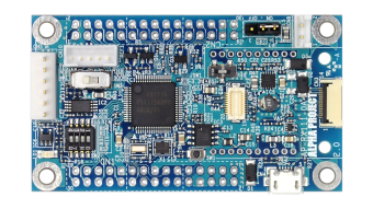
SoM/SBC
AP-RX111-0A
This high-performance and low-power CPU board equipped with the Renesas RX111 is well suited for prototyping and embedded device integration. Enables ultra-low-power operation and battery-powered designs, making it suitable for sensors, detectors, smart meters, and portable devices that require long-term operation on batteries. Supports the development of energy-efficient embedded systems for a wide range of low-power applications.
Supported Products:
RX111Provided By:
AlphaProject Co.,Ltd.Other
Reference Board for Motor Control Consulting Service
Provide Renesas CPU cards for inverter drive, as well as inverters enables with these CPU cards, ranging from low voltage to AC 400V, and from approximately 5A to 300A.
Supported Products:
RL78/F14,RL78/G1F,RL78/G1G,RL78/G14,RL78/G1M,RL78/F24,RX23T,RX24T,RX71M,RH850/F1KM-S1,RX13T,RX140,RH850/P1M,RX111,RA2E1,RX66T,RX72T,RZ/T1,RH850/P1M-E,RA6M1,RA6T1,RA6T2,RX26TProvided By:
Desk Top Lab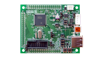
Evaluation
RX Family Microcontroller Board
This solution provides a general-purpose evaluation board featuring Renesas RX microcontrollers. It is available as a standalone evaluation board or as kit products supporting applications such as touch key interfaces and brushless motor control.
Supported Products:
RX110,RX111,RX113,RX130,RX140,RX13T,RX230,RX231,RX23E-A,RX23E-B,RX23T,RX24T,RX24U,RX260,RX261,RX26T,RX64M,RX65N,RX651,RX660,RX66N,RX66T,RX671,RX71M,RX72M,RX72N,RX72TProvided By:
HOKUTO DENSHI