
特長
- Fully Integrated PLL
- Up to 200 MHz I/O Frequency
- LVCMOS Outputs
- Outputs Disable in High Impedance
- LVCMOS Reference Clock Options
- LQFP Packaging
- 32-lead Pb-free Package Available
- ±50 ps Cycle-Cycle Jitter
- 150 ps Output Skews
説明
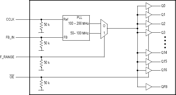
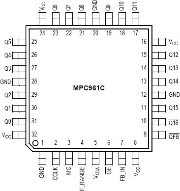
The MPC961 is offered with two different input configurations. The MPC961C offers an LVCMOS reference clock while the MPC961P offers an LVPECL reference clock. When pulled high the OE pin will force all of the outputs (except QFB) into a high impedance state. Because the OE pin does not affect the QFB output, down stream clocks can be disabled without the internal PLL losing lock. The MPC961 is fully 2.5 V or 3.3 V compatible and requires no external loop filter components. All control inputs accept LVCMOS compatible levels and the outputs provide low impedance LVCMOS outputs capable of driving terminated 50 ? transmission lines. For series terminated lines the MPC961 can drive two lines per output giving the device an effective fanout of 1:36. The device is packaged in a 32-lead LQFP.


